SLVS372C June 2001 – October 2015 TPS60240 , TPS60241 , TPS60242 , TPS60243
PRODUCTION DATA.
- 1 Features
- 2 Applications
- 3 Description
- 4 Revision History
- 5 Pin Configuration and Functions
- 6 Specifications
- 7 Detailed Description
- 8 Application and Implementation
- 9 Power Supply Recommendations
- 10Layout
- 11Device and Documentation Support
- 12Mechanical, Packaging, and Orderable Information
Package Options
Refer to the PDF data sheet for device specific package drawings
Mechanical Data (Package|Pins)
- DGK|8
Thermal pad, mechanical data (Package|Pins)
Orderable Information
7 Detailed Description
7.1 Overview
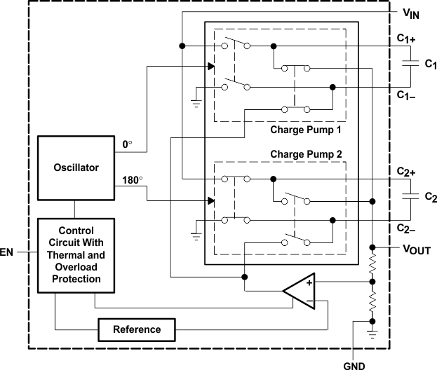
The TPS6024x device is a fixed-frequency, dual-phase charge pump that provides 25 mA of continuous supply current for low-noise applications such as VCOs used in mobile phones and wireless applications.
Low-noise operation results from using a proprietary dual-phase charge pump topology that relies on an operational amplifier in the feedback loop to reduce ripple. During the first phase, C1 is charged to the supply voltage. Pin C1+ is connected to VIN, and C1– is connected to GND. In the second phase, C1– is connected to the output of the operational amplifier, and C1+ is connected to VOUT. The operational amplifier then adjusts its output until the output VOUT delivers the correct voltage to make the resistor divided feedback point equal to the reference voltage. During this second phase, C2 is charged to supply voltage. Terminal C2– is connected to GND, and C2+ is connected to VIN. Phase one is then repeated with C2, now acting to provide charge to the output in place of C1, which is connected to the supply. The dual-phase operation lowers the output ripple voltage significantly compared to a standard single-phase charge pump. In addition, the linear feedback of the operational amplifier eliminates the ripple during discharge of the output capacitor (COUT).
7.2 Functional Block Diagram

7.3 Feature Description
7.3.1 Thermal Shutdown
The TPS6024x device has a built-in thermal shutdown which turns off the power stage when the junction temperature exceeds typical 160°C. When the junction temperature drops to typical 140°C, the device starts switching again.
7.3.2 Current Limit
The TPS6024x device has a built-in overload protection which limits the output current.
7.4 Device Functional Modes
7.4.1 Start-up Procedure
The converter is enabled when EN is set from logic low to high. The start-up time to reach 90% of the nominal output voltage is typically 0.5 ms at load currents lower than 10 mA and with an output capacitor of 1 µF. Increasing the values of COUT delays the start-up time.
7.4.2 Shutdown
Driving EN low disables the converter. This disables the internal circuits and reduces input current to typically 0.1 µA. In this mode, the load is disconnected from the supply voltage. The device exits shutdown once EN is set to a high level.