SLVSB50C December   2011  – June 2020 TPS61087-Q1

PRODUCTION DATA.  

  1. Features
  2. Applications
  3. Description
    1.     Device Images
      1.      Simplified Schematic
  4. Revision History
  5. Pin Configuration and Functions
    1.     Pin Functions
  6. Specifications
    1. 6.1 Absolute Maximum Ratings
    2. 6.2 ESD Ratings
    3. 6.3 Recommended Operating Conditions
    4. 6.4 Thermal Information
    5. 6.5 Electrical Characteristics
    6. 6.6 Typical Characteristics
  7. Detailed Description
    1. 7.1 Overview
    2. 7.2 Functional Block Diagram
    3. 7.3 Feature Description
      1. 7.3.1 Soft Start
      2. 7.3.2 Frequency Select Pin (FREQ)
      3. 7.3.3 Undervoltage Lockout (UVLO)
      4. 7.3.4 Thermal Shutdown
      5. 7.3.5 Overvoltage Prevention
    4. 7.4 Device Functional Modes
  8. Application and Implementation
    1. 8.1 Application Information
    2. 8.2 Typical Applications
      1. 8.2.1 Typical Application Circuit: 5 V to 15 V (fS = 1.2 MHz)
        1. 8.2.1.1 Design Requirements
        2. 8.2.1.2 Detailed Design Procedure
          1. 8.2.1.2.1 Inductor Selection
          2. 8.2.1.2.2 Rectifier Diode Selection
          3. 8.2.1.2.3 Setting the Output Voltage
          4. 8.2.1.2.4 Compensation (COMP)
          5. 8.2.1.2.5 Input Capacitor Selection
          6. 8.2.1.2.6 Output Capacitor Selection
      2. 8.2.2 Application Curves
      3. 8.2.3 Other Application Circuit Examples
  9. Power Supply Recommendations
  10. 10Layout
    1. 10.1 Layout Guidelines
    2. 10.2 Layout Example
  11. 11Device and Documentation Support
    1. 11.1 Device Support
      1. 11.1.1 Third-Party Products Disclaimer
    2. 11.2 Documentation Support
      1. 11.2.1 Related Documentation
    3. 11.3 Receiving Notification of Documentation Updates
    4. 11.4 Support Resources
    5. 11.5 Trademarks
    6. 11.6 Electrostatic Discharge Caution
    7. 11.7 Glossary
  12. 12Mechanical, Packaging, and Orderable Information

Package Options

Mechanical Data (Package|Pins)
Thermal pad, mechanical data (Package|Pins)
Orderable Information

Other Application Circuit Examples

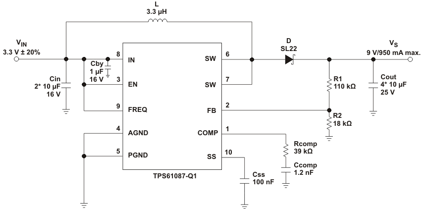
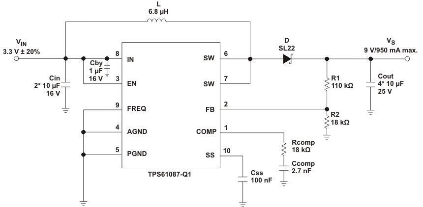
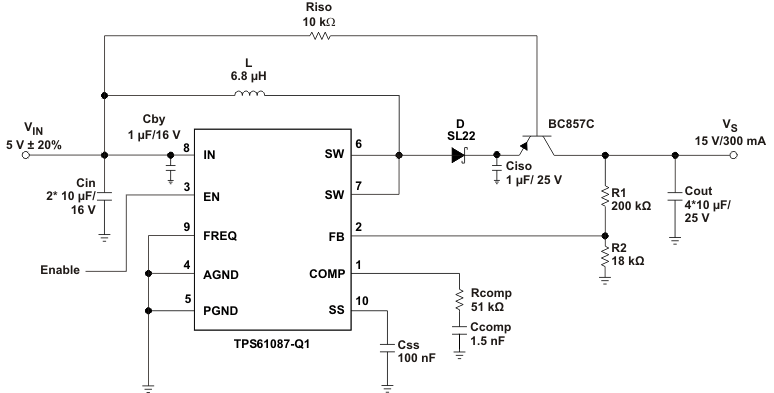
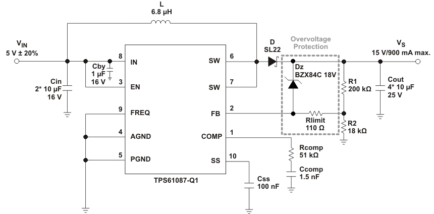
Figure 14 to Figure 22 show application circuit examples using the TPS61087-Q1 device. These circuits must be fully validated and tested by customers before using these circuits in their designs. TI does not warrant the accuracy or completeness of these circuits, nor does TI accept any responsibility for them.
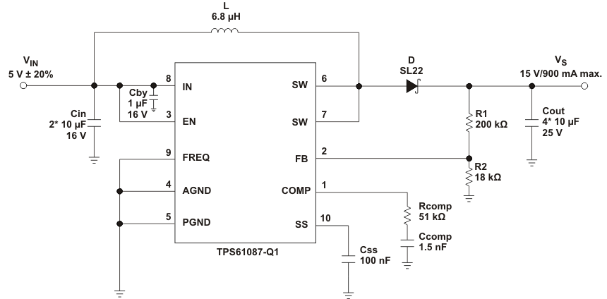
TPS61087-Q1 tapp2_lvsb50.gif
fS = 650 kHz VS = 15 V IOUT(max) = 900 mA
Figure 14. 5-V to 15-V Application Diagram
TPS61087-Q1 tapp3_lvsb50.gif
fS = 1.2 MHz VS = 9 V IOUT(max) = 950 mA
Figure 15. 3.3-V to 9-V Application Diagram
TPS61087-Q1 tapp4_lvsb50.gif
fS = 650 kHz VS = 9 V IOUT(max) = 950 mA
Figure 16. 3.3-V to 9-V Application Diagram
TPS61087-Q1 typ_app1_lvsb50.gif
fS = 650 kHz VS = 15 V IOUT = 300 mA
Figure 17. Diagram for Application With External Load Disconnect Switch
TPS61087-Q1 typ_app2_lvsb50.gif
fS = 650 kHz VS = 15 V IOUT(max) = 900 mA
Figure 18. Application Diagram for 5 V to 15 V With Overvoltage Protection
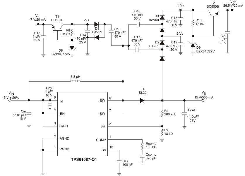
TPS61087-Q1 lcd_app_lvsb50.gif
fS = 1.2 MHz VS = 15 V IOUT = 500 mA
Figure 19. Application Diagram for 5 V to 15 V for TFT LCD With External Charge Pumps (VGH, VGL)
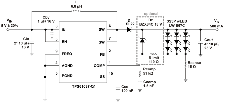
TPS61087-Q1 sim_app1_lvsb50.gif
fS = 650 kHz IOUT = 500 mA
Figure 20. Application Diagram for wLED Supply (3S3P) With Optional Clamping Zener Diode
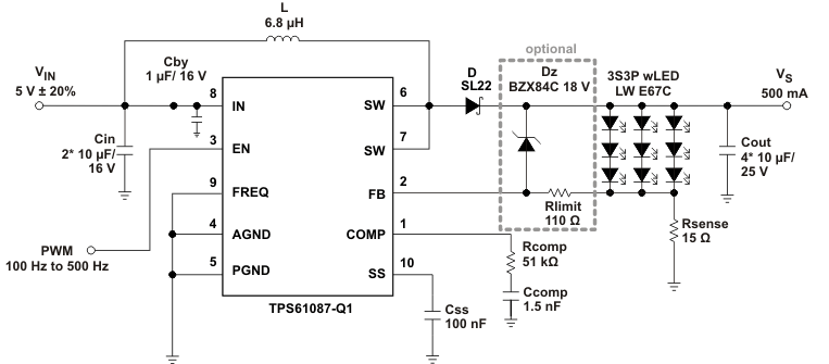
TPS61087-Q1 sim_app2_lvsb50.gif
fS = 650 kHz IOUT = 500 mA
Figure 21. Application Diagram for wLED Supply (3S3P) With Adjustable Brightness Control
Using A PWM Signal On The Enable Pin With Optional Clamping Zener Diode
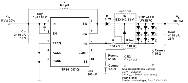
TPS61087-Q1 sim_app3_lvsb50.gif
fS = 650 kHz IOUT = 500 mA
Figure 22. Application Diagram for wLED Supply (3S3P) With Adjustable Brightness Control
Using An Analog Signal On The Feedback Pin With Optional Clamping Zener Diode