SLVSCF2A January 2014 – December 2014 TPS61097A-33
PRODUCTION DATA.
- 1 Features
- 2 Applications
- 3 Description
- 4 Revision History
- 5 Pin Configuration and Functions
- 6 Specifications
- 7 Parameter Measurement Information
- 8 Detailed Description
- 9 Application and Implementation
- 10Power Supply Recommendations
- 11Layout
- 12Device and Documentation Support
- 13Mechanical, Packaging, and Orderable Information
Package Options
Mechanical Data (Package|Pins)
- DBV|5
Thermal pad, mechanical data (Package|Pins)
Orderable Information
9 Application and Implementation
NOTE
Information in the following applications sections is not part of the TI component specification, and TI does not warrant its accuracy or completeness. TI’s customers are responsible for determining suitability of components for their purposes. Customers should validate and test their design implementation to confirm system functionality.
9.1 Application Information
9.1.1 Adjustable Bypass Switching
The EN pin can be set up as a low voltage control for the bypass switch. By setting the desired ratio of R1 and R2, the TPS61097A-33 can be set to switch on the bypass at a defined voltage level on VIN. For example, setting R1 and R2 to 200 KΩ would set VEN to half of VIN. The voltage level of VIN engaging the bypass switch is based on the VIL level of EN (0.58 V). If VIN is less than 1.16 V then the bypass switch will be enabled. For VIN values above 1.56 V (50% of VIH) the bypass switch is disabled.
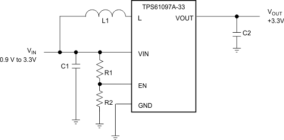 Figure 17. Adjustable Bypass Switching
9.1.2 Managing Inrush Current
Upon startup, the output capacitor of the boost converter can act as a virtual short circuit. The amount of inrush current is dependent on the rate of increase of the input voltage, the inductance used with the converter, the output capacitance and the parasitic circuit resistance. One method to reduce the inrush current is to use a load switch with controlled turn-on. Texas Instruments has a large offering of controlled slew rate load switches which can be found at www.ti.com/loadswitches. Below is an example circuit that has a load switch with controlled turn-on.
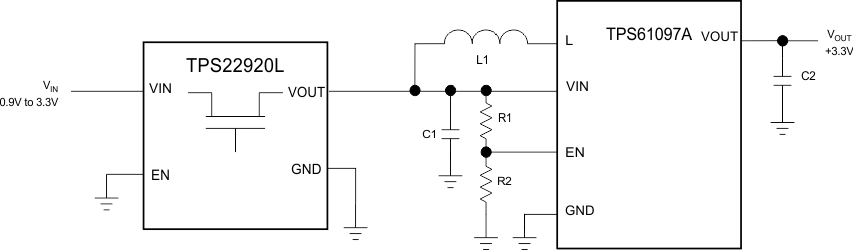 Figure 18. Example Circuit with Load Switch
9.1.3 Thermal Considerations
Implementation of integrated circuits in low-profile and fine-pitch surface-mount packages typically requires special attention to power dissipation. Many system-dependent issues such as thermal coupling, airflow, added heat sinks and convection surfaces, and the presence of other heat-generating components affect the power-dissipation limits of a given component.
Three basic approaches for enhancing thermal performance are listed below.
- Improving the power dissipation capability of the PCB design
- Improving the thermal coupling of the component to the PCB
- Introducing airflow in the system
The maximum recommended junction temperature (TJ) of the TPS61097A-33 devices is 125°C. Specified regulator operation is assured to a maximum ambient temperature TA of 85°C. Therefore, the maximum power dissipation is about 191.7 mW. More power can be dissipated if the maximum ambient temperature of the application is lower.
9.2 Typical Application
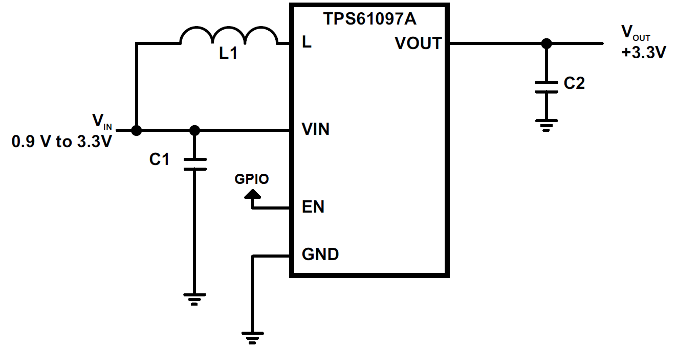 Figure 19. Typical Application Schematic
9.2.1 Design Requirements
| DESIGN PARAMETERS | EXAMPLE VALUE |
|---|---|
| Input Voltage (VIN) | 1.2 V to 1.8 V |
| Output Voltage (VOUT) | 3.3 V |
| Output Current (IOUT) | 10 mA |
9.2.2 Detailed Design Procedure
9.2.2.1 Inductor Selection
To make sure that the TPS61097A-33 devices can operate, a suitable inductor must be connected between pin VIN and pin L. Inductor values of 4.7 μH show good performance over the whole input and output voltage range .
Choosing other inductance values affects the switching frequency f proportional to 1/L as shown in Equation 1.
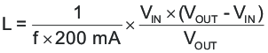
Choosing inductor values higher than 4.7 μH can improve efficiency due to reduced switching frequency and therefore with reduced switching losses. Using inductor values below 2.2 μH is not recommended.
Having selected an inductance value, the peak current for the inductor in steady state operation can be calculated. Equation 2 gives the peak current estimate.
IL,MAX is the inductor's required minimum current rating. Note that load transient or over current conditions may require an even higher current rating.
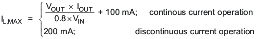
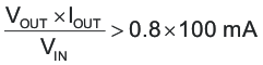
Equation 3 provides an easy way to estimate whether the device is operating in continuous or discontinuous operation. As long as the equation is true, continuous operation is typically established. If the equation becomes false, discontinuous operation is typically established.
Due to the use of current hysteretic control in the TPS61097A-33, the series resistance of the inductor can impact the operation of the main switch. There is a simple calculation that can ensure proper operation of the TPS61097A-33 boost converter. The relationship between the series resistance (RIN), the input voltage (VIN) and the switch current limit (ISW) is shown in Equation 4.
Examples:
In Equation 5, RIN < 2.5 V / 400 mA; therefore, RIN must be less than 6.25 Ω.
In Equation 6, RIN < 1.8 V / 400 mA; therefore, RIN must be less than 4.5 Ω.
The following inductor series from different suppliers have been used with TPS61097A-33 converters:
Table 2. List of Inductors
| VENDOR | INDUCTOR SERIES |
|---|---|
| Coilcraft | DO3314 |
| TDK | NLC565050T |
| Taiyo Yuden | CBC2012T |
9.2.2.2 Capacitor Selection
9.2.2.2.1 Input Capacitor
The input capacitor should be at least 10-μF to improve transient behavior of the regulator and EMI behavior of the total power supply circuit. The input capacitor should be a ceramic capacitor and be placed as close as possible to the VIN and GND pins of the IC.
9.2.2.2.2 Output Capacitor
For the output capacitor C2, it is recommended to use small ceramic capacitors placed as close as possible to the VOUT and GND pins of the IC. If, for any reason, the application requires the use of large capacitors which can not be placed close to the IC, the use of a small ceramic capacitor with a capacitance value of around 2.2 μF in parallel to the large one is recommended. This small capacitor should be placed as close as possible to the VOUT and GND pins of the IC.
A minimum capacitance value of 4.7 μF should be used, 10 μF are recommended. If the inductor exceeds 4.7 μH, the value of the output capacitance value needs to be half the inductance value or higher for stability reasons, see Equation 7.

Using low ESR capacitors, such as ceramic capacitors, is recommended to minimize output voltage ripple. If heavy load changes are expected, the output capacitor value should be increased to avoid output voltage drops during fast load transients.
Table 3. Recommended Output Capacitors
| VENDOR | CAPACITOR SERIES |
|---|---|
| Murata | GRM188R60J106M47D 10μF 6.3V X5R 0603 |
| Murata | GRM319R61A106KE19 10μF 10V X5R 1206 |
9.2.3 Application Curves
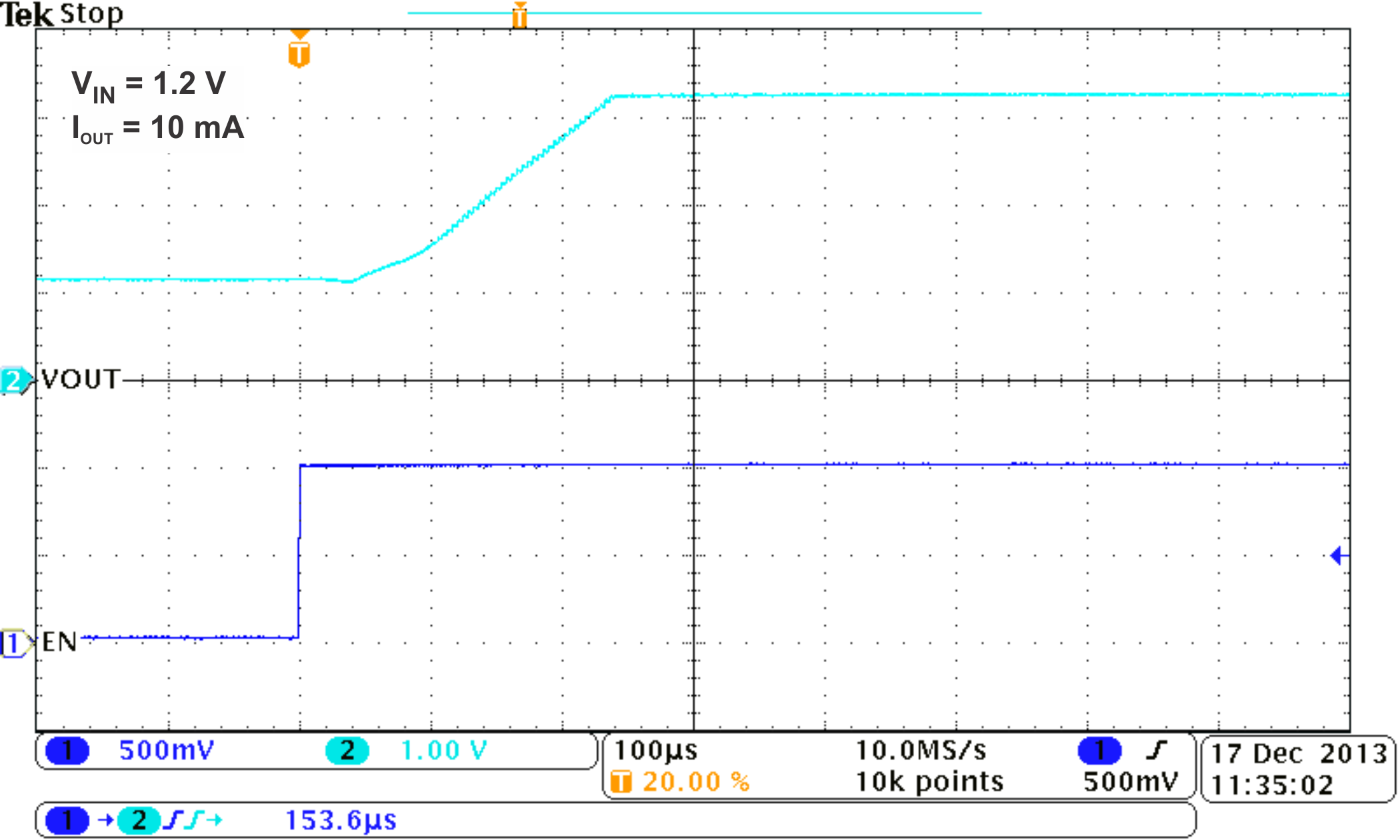
| VIN = 1.2 V | ||
| IOUT = 10 mA |
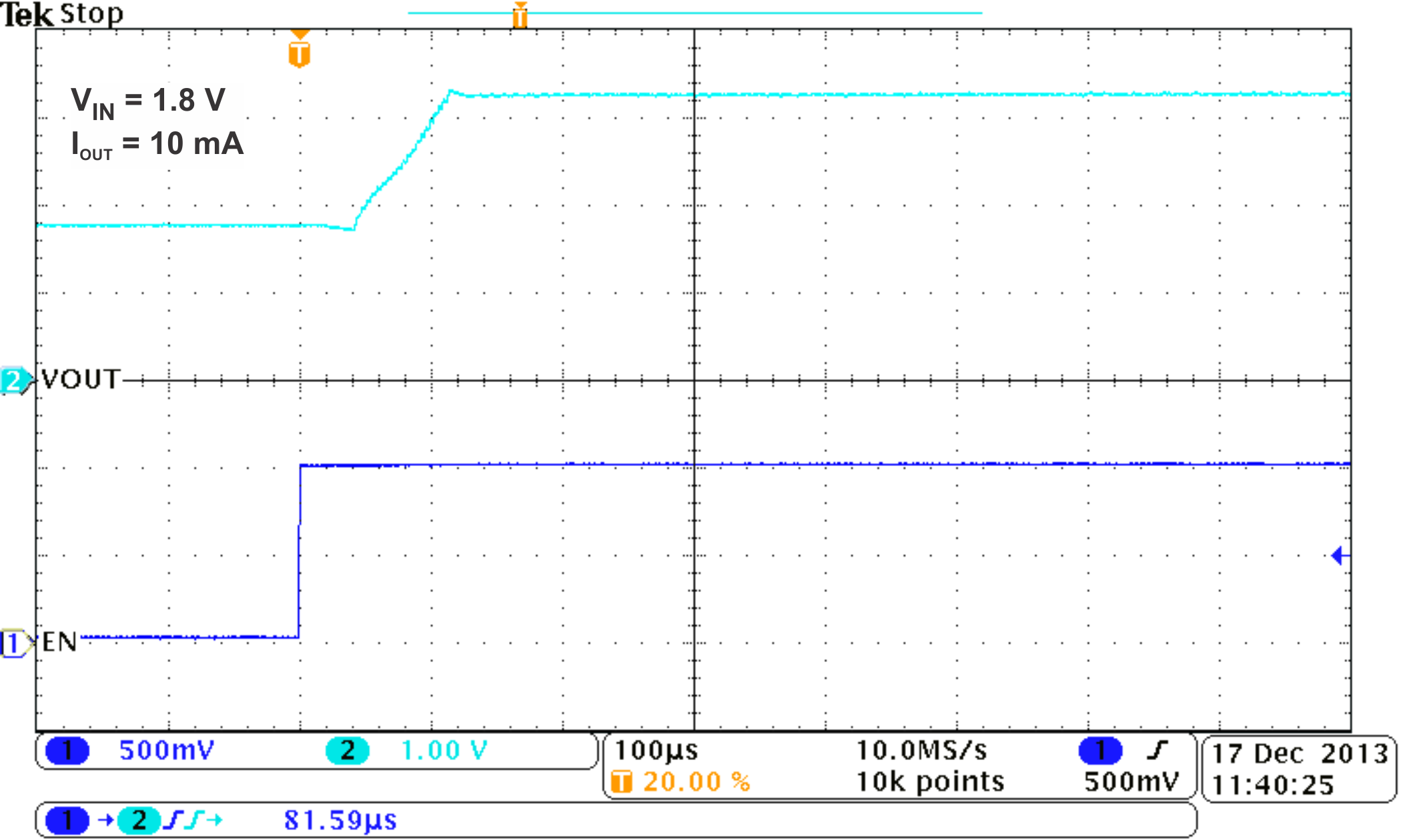
| VIN = 1.8 V | ||
| IOUT = 1.8 mA |