SLVSCF2A January 2014 – December 2014 TPS61097A-33
PRODUCTION DATA.
- 1 Features
- 2 Applications
- 3 Description
- 4 Revision History
- 5 Pin Configuration and Functions
- 6 Specifications
- 7 Parameter Measurement Information
- 8 Detailed Description
- 9 Application and Implementation
- 10Power Supply Recommendations
- 11Layout
- 12Device and Documentation Support
- 13Mechanical, Packaging, and Orderable Information
Package Options
Mechanical Data (Package|Pins)
- DBV|5
Thermal pad, mechanical data (Package|Pins)
Orderable Information
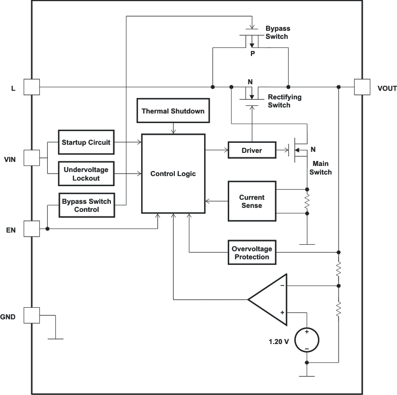
8 Detailed Description
8.1 Overview
The TPS61097A-33 is a high performance, high efficiency switching boost converter. To achieve high efficiency the power stage is realized as a synchronous boost topology. For the power switching, two actively controlled low RDSon power MOSFETs are implemented.
8.2 Functional Block Diagram
8.3 Feature Description
8.3.1 Controller Circuit
The device is controlled by a hysteretic current mode controller. This controller regulates the output voltage by keeping the inductor ripple current constant in the range of 200 mA and adjusting the offset of this inductor current depending on the output load. If the required average input current is lower than the average inductor current defined by this constant ripple the inductor current goes discontinuous to keep the efficiency high at low load conditions.
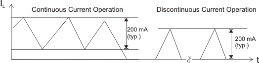 Figure 16. Hysteretic Current Operation
The output voltage VOUT is monitored via the feedback network which is connected to the voltage error amplifier. To regulate the output voltage, the voltage error amplifier compares this feedback voltage to the internal voltage reference and adjusts the required offset of the inductor current accordingly.
8.3.2 Device Enable and Shutdown Mode
The device is enabled when EN is set high and shut down when EN is low. During shutdown, the converter stops switching and all internal control circuitry is turned off.
8.3.3 Bypass Switch
The TPS61097A-33 contains a P-channel MOSFET (Bypass Switch) in parallel with the synchronous rectifying MOSFET. When the IC is enabled (VEN > VIH), the Bypass Switch is turned off to allow the IC to work as a standard boost converter. When the IC is disabled (VEN < VIL) the Bypass Switch is turned on to provide a direct, low impedance connection from the input voltage (at the L pin) to the load (VOUT). The Bypass Switch is not impacted by Undervoltage lockout, Overvoltage or Thermal shutdown.
8.3.4 Startup
After the EN pin is tied high, the device starts to operate. If the input voltage is not high enough to supply the control circuit properly a startup oscillator starts to operate the switches. During this phase the switching frequency is controlled by the oscillator and the maximum switch current is limited. As soon as the device has built up the output voltage to about 1.8 V, high enough for supplying the control circuit, the device switches to its normal hysteretic current mode operation. The startup time depends on input voltage and load current.
8.3.5 Operation at Output Overload
If in normal boost operation the inductor current reaches the internal switch current limit threshold the main switch is turned off to stop further increase of the input current. In this case the output voltage will decrease since the device can not provide sufficient power to maintain the set output voltage.
If the output voltage drops below the input voltage the backgate diode of the rectifying switch gets forward biased and current starts flow through it. Because this diode cannot be turned off, the load current is only limited by the remaining DC resistances. As soon as the overload condition is removed, the converter automatically resumes normal operation and enters the appropriate soft start mode depending on the operating conditions.
8.3.6 Undervoltage Lockout
An undervoltage lockout function stops the operation of the converter if the input voltage drops below the typical undervoltage lockout threshold. This function is implemented in order to prevent malfunctioning of the converter. The undervoltage lockout function has no control of the Bypass Switch. If the Bypass Switch is enabled
(VEN < VIL) there is no impact during an undervoltage condition, and the Bypass Switch remains on.
8.3.7 Overtemperature Protection
The device has a built-in temperature sensor which monitors the internal IC temperature. If the temperature exceeds the programmed threshold (OTP), the device stops operating. As soon as the IC temperature has decreased below the programmed threshold (OTP - OTP HYST), it starts operating again. There is a built-in hysteresis to avoid unstable operation at IC temperatures at the overtemperature threshold.
8.4 Device Functional Modes
| EN | DEVICE STATE |
|---|---|
| H | Boost Converter |
| L | Bypass Switch |