SNVSA79 March 2015 TPS61196-Q1
PRODUCTION DATA.
- 1 Features
- 2 Applications
- 3 Description
- 4 Revision History
- 5 Pin Configuration and Functions
- 6 Specifications
-
7 Detailed Description
- 7.1 Overview
- 7.2 Functional Block Diagram
- 7.3 Feature Description
- 7.4
Device Functional Modes
- 7.4.1
Protections
- 7.4.1.1 Switch Current Limit Protection Using the ISNS Pin
- 7.4.1.2 LED Open Protection
- 7.4.1.3 LED Short-Cross Protection Using the FBP Pin
- 7.4.1.4 Schottky Diode Open Protection
- 7.4.1.5 Schottky Diode Short Protection
- 7.4.1.6 IFB Overvoltage Protection During Start-up
- 7.4.1.7 Output Overvoltage Protection Using the OVP Pin
- 7.4.1.8 Output Short-to-Ground Protection
- 7.4.1.9 IFB Short-to-Ground Protection
- 7.4.1.10 ISET Short-to-Ground Protection
- 7.4.1.11 Thermal Protection
- 7.4.2 Indication For Fault Conditions
- 7.4.1
Protections
- 8 Application and Implementation
- 9 Power Supply Recommendations
- 10Layout
- 11Device and Documentation Support
- 12Mechanical, Packaging, and Orderable Information
Package Options
Mechanical Data (Package|Pins)
- PWP|28
Thermal pad, mechanical data (Package|Pins)
- PWP|28
Orderable Information
10 Layout
10.1 Layout Guidelines
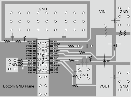
As for all switching power supplies, especially those providing high current and using high switching frequencies, layout is an important design step. If layout is not carefully done, the regulator could show instability as well as EMI problems. Therefore, use wide and short traces for high current paths. The VDD capacitor, C3 (see Figure 22) is the filter and noise decoupling capacitor for the internal linear regulator powering the internal digital circuits. It should be placed as close as possible between the VDD and PGND pins to prevent any noise insertion to digital circuits. The switch node at the drain of Q1 carries high current with fast rising and falling edges. Therefore, the connection between this node to the inductor and the Schottky diode should be kept as short and wide as possible. It is also beneficial to have the ground of the capacitor C3 close to the ground of the current sense resistor R7 since there is large driving current flowing between them. The ground of output capacitor EC2 should be kept close to input power ground or through a large ground plane because of the large ripple current returning to the input ground. When laying out signal grounds, it is recommended to use short traces separate from power ground traces and connect them together at a single point, for example on the thermal pad in the PWP package. Resistors R3, R4, R9, R10, R11, and R12 (see Figure 22) are setting resistors for switching frequency, LED current, protection threshold and feedback voltage programming. To avoid unexpected noise coupling into the pins and affecting the accuracy, these resistors need to be close to the pins with short and wide traces to GND. In the PWP package, the thermal pad needs to be soldered to the large ground plane on the PCB for better thermal performance. Additional thermal via can significantly improve power dissipation of the device.
10.2 Layout Example
 Figure 27. Layout Example