SNVSA79 March 2015 TPS61196-Q1
PRODUCTION DATA.
- 1 Features
- 2 Applications
- 3 Description
- 4 Revision History
- 5 Pin Configuration and Functions
- 6 Specifications
-
7 Detailed Description
- 7.1 Overview
- 7.2 Functional Block Diagram
- 7.3 Feature Description
- 7.4
Device Functional Modes
- 7.4.1
Protections
- 7.4.1.1 Switch Current Limit Protection Using the ISNS Pin
- 7.4.1.2 LED Open Protection
- 7.4.1.3 LED Short-Cross Protection Using the FBP Pin
- 7.4.1.4 Schottky Diode Open Protection
- 7.4.1.5 Schottky Diode Short Protection
- 7.4.1.6 IFB Overvoltage Protection During Start-up
- 7.4.1.7 Output Overvoltage Protection Using the OVP Pin
- 7.4.1.8 Output Short-to-Ground Protection
- 7.4.1.9 IFB Short-to-Ground Protection
- 7.4.1.10 ISET Short-to-Ground Protection
- 7.4.1.11 Thermal Protection
- 7.4.2 Indication For Fault Conditions
- 7.4.1
Protections
- 8 Application and Implementation
- 9 Power Supply Recommendations
- 10Layout
- 11Device and Documentation Support
- 12Mechanical, Packaging, and Orderable Information
Package Options
Mechanical Data (Package|Pins)
- PWP|28
Thermal pad, mechanical data (Package|Pins)
- PWP|28
Orderable Information
6 Specifications
6.1 Absolute Maximum Ratings(1)
over operating free-air temperature range (unless otherwise noted)| MIN | MAX | UNIT | ||
|---|---|---|---|---|
| Voltage(2) | VIN pin | –0.3 | 33 | V |
| FAULT pin | –0.3 | VIN | ||
| FB1 to IFB6 pins | –0.3 | 40 | ||
| FBP, ISET, ISNS, IFBV pins | –0.3 | 3.3 | ||
| EN, PWM1 to PWM6 pins | –0.3 | 20 | ||
| GDRV pins | –0.3 | 7 | ||
| GDRV 10-ns transient pins | –2 | 9 | ||
| All other pins | –0.3 | 7 | ||
| Continuous power dissipation | See Thermal Information | |||
| Operating junction temperature range | –40 | 150 | °C | |
| Storage temperature, Tstg | –65 | 150 | °C | |
(1) Stresses beyond those listed under Absolute Maximum Ratings may cause permanent damage to the device. These are stress ratings only, which do not imply functional operation of the device at these or any other conditions beyond those indicated under Recommended Operating Conditions. Exposure to absolute-maximum-rated conditions for extended periods may affect device reliability.
(2) All voltage values are with respect to network ground terminal
6.2 ESD Ratings
| VALUE | UNIT | |||
|---|---|---|---|---|
| V(ESD) | Electrostatic discharge | Human-body model (HBM), per AEC Q100-002(1) | ±2000 | V |
| Charged-device model (CDM), per AEC Q100-011 | ±750 | |||
(1) AEC Q100-002 indicates that HBM stressing shall be in accordance with the ANSI/ESDA/JEDEC JS-001 specification.
6.3 Recommended Operating Conditions
over operating free-air temperature range (unless otherwise noted)(1)| MIN | NOM | MAX | UNIT | ||
|---|---|---|---|---|---|
| VIN | Input voltage | 8 | 30 | V | |
| VOUT | Output voltage | VIN | 120 | V | |
| L1 | Inductor | 10 | 100 | µH | |
| CIN | Input capacitor | 10 | µF | ||
| COUT | Output capacitor | 22 | 220 | µF | |
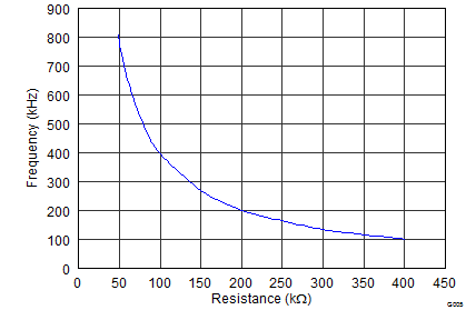
| fSW | Boost regulator switching frequency | 100 | 800 | kHz | |
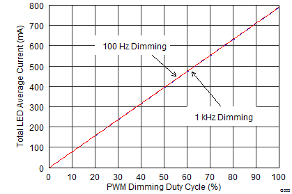
| fDIM | PWM dimming frequency | 0.09 | 22 | kHz | |
| TA | Operating ambient temperature | –40 | 125 | °C | |
| TJ | Operating junction temperature | –40 | 125 | °C |
(1) Customers need to verify the component value in their application if the values are different from the recommended values.
6.4 Thermal Information
| THERMAL METRIC(1) | PWP (HTSSOP) | UNIT | |
|---|---|---|---|
| 28 PINS | |||
| RθJA | Junction-to-ambient thermal resistance | 33.8 | °C/W |
| RθJC(top) | Junction-to-case (top) thermal resistance | 18.8 | |
| RθJB | Junction-to-board thermal resistance | 15.6 | |
| ψJT | Junction-to-top characterization parameter | 0.6 | |
| ψJB | Junction-to-board characterization parameter | 15.4 | |
| RθJC(bot) | Junction-to-case (bottom) thermal resistance | 2.5 | |
(1) For more information about traditional and new thermal metrics, see the IC Package Thermal Metrics application report, SPRA953.
6.5 Electrical Characteristics
VIN= 24 V, C1 = 10 μF, C2 = 2.2 μF, C3 = 1 μF, EC1 = EC2 = 100 μF; Typical values are at TA = 25°C, Minimum and Maximum limits are over the operating temperature range (TA = –40°C to 125°C) (unless otherwise noted).| PARAMETER | TEST CONDITIONS | MIN | TYP | MAX | UNIT | |
|---|---|---|---|---|---|---|
| POWER SUPPLY | ||||||
| VIN | Input voltage range | 8 | 30 | V | ||
| VVIN_UVLO | Undervoltage lockout threshold | VIN falling | 6.5 | 7 | V | |
| VVIN_HYS | VIN UVLO hysteresis | 300 | mV | |||
| Iq_VIN | Operating quiescent current into VIN | Device enabled, no switching, VIN = 30 V | 2 | mA | ||
| ISD | Shutdown current | VIN = 12 V, VIN = 30 V |
25 50 |
µA | ||
| VDD | Regulation voltage for internal circuit | 0 mA < IDD < 15 mA | 5.7 | 6 | 6.3 | V |
| EN and PWMx | ||||||
| VH | Logic high input on EN,PWMx | VIN = 8 V to 30 V | 1.8 | V | ||
| VL | Logic Low input on EN, PWMx | VIN = 8 V to 30 V | 0.8 | V | ||
| RPD | Pull-down resistance on EN, PWMx | 0.8 | 1.6 | 3 | MΩ | |
| UVLO | ||||||
| VUVLOTH | Threshold voltage at UVLO pin | 1.204 | 1.229 | 1.253 | V | |
| IUVLO | UVLO input bias current | VUVLO = VUVLOTH – 50 mV VUVLO = VUVLOTH + 50 mV |
–0.1 –4.3 |
-3.9 |
0.1 –3.3 |
µA |
| SOFT START | ||||||
| ISS | Soft start charging current | PWM ON, VREF< 2 V PWM ON, VREF> 2 V |
200 10 |
µA | ||
| CURRENT REGULATION | ||||||
| VISET | ISET pin voltage | 1.217 | 1.229 | 1.240 | V | |
| IISET_P | ISET short-to-ground protection threshold | 120 | 150 | 180 | µA | |
| KISET | Current multiple IIFB/IISET | IISET = 32.56 µA, VIFB = 0.5 V | 3932 | 3992 | 4052 | |
| IIFB(AVG) | Current accuracy | IISET = 32.56 µA, VIFB = 0.5 V | 127.4 | 130 | 132.6 | mA |
| KIFB(M) | Current matching; (IFB(MAX)– IFB(MIN))/2IFB(AVG) | IISET = 32.56 µA, VIFB = 0.5 V | 0.5% | 1.5% | ||
| IIFB_LEAK | IFB pin leakage current at dimming off | IFB voltage < 40 V | 1 | µA | ||
| IIFB_max | Current sink max output current | VIFBV = 350 mV | 130 | mA | ||
| IFB REGULATION VOLTAGE | ||||||
| VIFB | Regulation voltage at IFB | Measured on VIFB(min), other IFB voltages are 0.5 V above VIFB(min). IIFB = 130 mA, VIFBV = 0.5 V |
508 | mV | ||
| IIFBV | IFB Regulation voltage setting sourcing current at IFBV | VIFBV = 0.5 V | 0.247 | 0.25 | 0.253 | IISET |
| VIFBV | IFBV voltage setting range | 0.3 | 1 | V | ||
| BOOST REFERENCE VOLTAGE | ||||||
| VREF | Reference voltage range for Boost Controller | 0 | 3.1 | V | ||
| IREF_LEAK | Leakage current at REF pin | –25 | 25 | nA | ||
| OSCILLATOR | ||||||
| fSW | Switching frequency | RFSW = 200 kΩ | 187 | 200 | 213 | kHz |
| VFSW | FSW pin reference voltage | 1.8 | V | |||
| Dmax | Maximum duty cycle | fSW = 200 kHz | 90% | 94% | 98% | |
| ton(min) | Minimum pulse width | 200 | ns | |||
| VFSW_H | Logic high input voltage | 3.5 | V | |||
| VFSW_L | Logic low input voltage | 0.5 | V | |||
| ERROR AMPLIFIER | ||||||
| ISINK | Comp pin sink current | VOVP = VREF + 200 mV, VCOMP = 1 V | 20 | µA | ||
| ISOURCE | Comp pin source current | VOVP = VREF – 200 mV, VCOMP = 1 V | 20 | µA | ||
| GmEA | Error amplifier transconductance | 90 | 120 | 150 | µs | |
| REA | Error amplifier output resistance | 20 | MΩ | |||
| fEA | Error amplifier crossover frequency | 1000 | kHz | |||
| GATE DRIVER | ||||||
| RGDRV(SRC) | Gate driver impedance when sourcing | VDD = 6 V, IGDRV = –20 mA | 2 | 3 | Ω | |
| RGDRV(SNK) | Gate driver impedance when sinking | VDD = 6 V, IGDRV = 20 mA | 1 | 1.5 | Ω | |
| IGDRV(SRC) | Gate driver source current | VGDRV = 5 V | 200 | mA | ||
| IGDRV(SNK) | Gate driver sink current | VGDRV = 1 V | 400 | mA | ||
| VISNS(OC) | Overcurrent detection threshold | VIN = 8 V to 30 V, TJ = 25°C to 125°C | 376 | 400 | 424 | mV |
| OVERVOLTAGE PROTECTION (OVP) | ||||||
| VOVPTH | Output voltage OVP threshold | 2.95 | 3.02 | 3.09 | V | |
| IOVP | Leakage current | –100 | 0 | 100 | nA | |
| VIFB_OVP | IFBx over voltage threshold | PWM ON | 38 | V | ||
| LED SHORT DETECTION | ||||||
| IFBP | LED short detection sourcing current | VFBP = 1 V | 0.247 | 0.25 | 0.253 | IISET |
| FAULT INDICATOR | ||||||
| IFAULT_H | Leakage current in high impedance | VFAULT = 24 V | 1 | nA | ||
| IFAULT_L | Sink current at low output | VFAULT = 1 V | 1 | 2 | mA | |
| THERMAL SHUTDOWN | ||||||
| Tshutdown | Thermal shutdown threshold | 150 | °C | |||
| Thys | Thermal shutdown threshold hysteresis | 15 | °C | |||
6.6 Typical Characteristics
