SLVSCM3B january 2015 – august 2023 TPS62065-Q1 , TPS62067-Q1
PRODUCTION DATA
- 1
- 1 Features
- 2 Applications
- 3 Description
- 4 Revision History
- 5 Device Comparison Table
- 6 Pin Configuration and Functions
- 7 Specifications
- 8 Parameter Measurement Information
-
9 Detailed Description
- 9.1 Overview
- 9.2 Functional Block Diagram
- 9.3
Feature Description
- 9.3.1 Mode Selection (TPS62065-Q1) and Forced PWM Mode (TPS62067A-Q1)
- 9.3.2 Power Good (PG, TPS62067x-Q1)
- 9.3.3 Enable
- 9.3.4 Shutdown and Output Discharge
- 9.3.5 Soft Start
- 9.3.6 Undervoltage Lockout (UVLO)
- 9.3.7 Internal Current Limit and Foldback Current Limit For Short-Circuit Protection
- 9.3.8 Clock Dithering
- 9.3.9 Thermal Shutdown
- 9.4 Device Functional Modes
- 10Application and Implementation
- 11Device and Documentation Support
- 12Mechanical, Packaging, and Orderable Information
Package Options
Mechanical Data (Package|Pins)
- DSG|8
Thermal pad, mechanical data (Package|Pins)
- DSG|8
Orderable Information
3 Description
The TPS62065-Q1, TPS62067-Q1, and TPS62067A-Q1 devices are highly-efficient, synchronous, step-down DC/DC converters. The device provides up to 2-A output current.
With an input voltage range of 2.9 V to 6 V the device is an excellent fit for power conversion from a 5-V or 3.3-V system supply rail. The TPS62065-Q1 and TPS62067-Q1 device operates at 3-MHz fixed frequency and enters power-save mode operation at light load currents to maintain high efficiency over the entire load current range. The power save mode is optimized for low output-voltage ripple. For low noise applications, the TPS62065-Q1 device can be forced into fixed frequency PWM mode by pulling the MODE pin high. The TPS62067-Q1 provides an open drain power good output and has a power save mode, while the TPS62067A-Q1 operates in fixed frequency PWM mode. In the shutdown mode, the current consumption is reduced to 5 µA and an internal circuit discharges the output capacitor. The TPS62065-Q1, TPS62067-Q1, and TPS62067A-Q1 devices are optimized for operation with a tiny 1-µH inductor and a small 10-µF output capacitor to achieve smallest design size and high regulation performance.
The new product, TPS628502-Q1, offers reduced BOM cost and size, higher efficiency and other features.
| PART NUMBER | PACKAGE(1) | PACKAGE SIZE(2) |
|---|---|---|
| TPS62065-Q1, TPS62067-Q1, TPS62067A-Q1 | DSG (WSON, 8) | 2.00 mm × 2.00 mm × 0.80 mm |
 Typical Application
Circuit
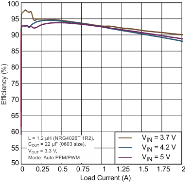
 Efficiency vs Load
Current