SLVSC20E January 2015 – October 2016 TPS62134A , TPS62134B , TPS62134C , TPS62134D
PRODUCTION DATA.
- 1 Features
- 2 Applications
- 3 Description
- 4 Revision History
- 5 Device Comparison Table
- 6 Pin Configuration and Functions
- 7 Specifications
-
8 Detailed Description
- 8.1 Overview
- 8.2 Functional Block Diagram
- 8.3
Feature Description
- 8.3.1 Enable and Shutdown (EN)
- 8.3.2 Undervoltage Lockout (UVLO)
- 8.3.3 Soft-Start (SS) Circuitry
- 8.3.4 Switch Current-Limit and Short Circuit Protection
- 8.3.5 Output Voltage and LPM Logic Selection (VIDx and LPM)
- 8.3.6 Power-Good Output (PG)
- 8.3.7 Single-Ended Remote Sense (FBS)
- 8.3.8 Thermal Shutdown
- 8.4 Device Functional Modes
- 9 Application and Implementation
- 10Power Supply Recommendations
- 11Layout
- 12Device and Documentation Support
- 13Mechanical, Packaging, and Orderable Information
Package Options
Mechanical Data (Package|Pins)
- RGT|16
Thermal pad, mechanical data (Package|Pins)
- RGT|16
Orderable Information
1 Features
- DCS-Control™ Architecture
- Supports Low-Power Mode for System Standby Mode
- Power Save Mode for Light Load Efficiency
- Selectable Fixed Output Voltage (0.7 V to 1.05 V)
- Low Power Mode Logic Input
- Quiescent Current of 20 µA
- Input Voltage Range: 3 V to 17 V
- Output Current: up to 3.2 A
- Programmable Soft Start
- Power Good Output
- Short Circuit Protection
- Single-ended Remote Sense
- Thermal Shutdown Protection
- Available in a 3-mm × 3-mm, VQFN-16 Package
2 Applications
- Intel Skylake™ Platform Ultrabook, Notebook, PC
- Standard 12-V Rail Supply
- POL Supply from 1 to 4 Cells Li-Ion Battery
- Solid-State Disk Drive
- Embedded System
3 Description
The TPS62134x family of devices is an easy-to-use, synchronous step-down DC-DC converter, compatible with Intel Skylake platform applications such as Ultrabooks™ and notebooks. The high performance DCS-Control™ architecture provides fast transient response as well as high output voltage accuracy.
With a wide operating input-voltage range of 3 to 17 V, the devices are ideally suited for systems powered from either a Li-Ion or other batteries as well as from 12-V intermediate power rails. The devices have a low-power mode where the output voltage is reduced by using the LPM pin. In addition, the devices support dynamic output-voltage change by using the VIDx pins. The LPM and VIDx pins help the system minimize power consumption in different operating modes.
The output-voltage startup ramp is controlled by the SS pin. The power sequencing is configurable by the enable (EN) and power good (PG) pins. In power-save mode, the devices show quiescent current of approximately 20 μA which maintains high efficiency over the entire load range. Short circuit protection and thermal shutdown protect the IC and external components from heavy current when the output is shorted to ground. The device is available in a 3-mm × 3-mm 16-pin VQFN package with thermal pad.
Device Information(1)
| PART NUMBER | PACKAGE | BODY SIZE (NOM) |
|---|---|---|
| TPS62134A | VQFN | 3.00mm x 3.00mm |
| TPS62134B | ||
| TPS62134C | ||
| TPS62134D |
- For all available packages, see the orderable addendum at the end of the data sheet.
spacer
spacer
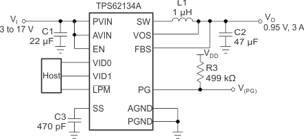
Typical Application Circuit

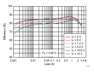
TPS62134A Efficiency
