SLVSBH3B June 2016 – April 2017 TPS62135
PRODUCTION DATA.
- 1 Features
- 2 Applications
- 3 Description
- 4 Revision History
- 5 Device Comparison Table
- 6 Pin Configuration and Functions
- 7 Specifications
- 8 Parameter Measurement Information
-
9 Detailed Description
- 9.1 Overview
- 9.2 Functional Block Diagram
- 9.3 Feature Description
- 9.4
Device Functional Modes
- 9.4.1 Pulse Width Modulation (PWM) Operation
- 9.4.2 Power Save Mode Operation (PWM/PFM)
- 9.4.3 100% Duty-Cycle Operation
- 9.4.4 HICCUP Current Limit And Short Circuit Protection (TPS62135 only)
- 9.4.5 Current Limit And Short Circuit Protection (TPS621351 only)
- 9.4.6 Soft-Start / Tracking (SS/TR)
- 9.4.7 Output Discharge Function (TPS62135 only)
- 9.4.8 Starting into a Pre-Biased Load (TPS621351 only)
- 10Application and Implementation
- 11Power Supply Recommendations
- 12Layout
- 13Device and Documentation Support
- 14Mechanical, Packaging, and Orderable Information
Package Options
Mechanical Data (Package|Pins)
- RGX|11
Thermal pad, mechanical data (Package|Pins)
Orderable Information
1 Features
- Output Voltage Accuracy ± 1% (PWM mode)
- Input Voltage Range: 3 V to 17 V
- Quiescent Current 18 µA Typ
- Output Voltage from 0.8 V to 12 V
- Adjustable Soft-Start
- Forced PWM or PWM/PFM operation
- Typical switching frequency of 2.5MHz in forced PWM
- Precise ENABLE input allows
- User-Defined Undervoltage Lockout
- Exact Sequencing
- 100% Duty Cycle Mode
- Automatic Efficiency Enhancement AEE™
- DCS-Control™ Topology
- Available with Active Output Discharge
- Optional HICCUP Overcurrent Protection
- Power Good Output
- Available in 3-mm x 2-mm VQFN Package
2 Applications
- Standard 12-V Rail Supplies
- POL for Connected Standby Requirements
- POL Supply from Single or Multiple Li-Ion Battery
- Gaming Consoles, SSD Drives
- Mobile and Embedded Computers
3 Description
The TPS62135 and TPS621351 are high efficiency and easy to use synchronous step-down DC-DC converters, based on the DCS-Control™ Topology. The devices wide input voltage range of 3-V to 17-V makes it suitable for multi-cell Li-Ion as well as 12-V intermediate supply rails. The devices provide 4-A continuous output current. The TPS62135 automatically enters Power Save Mode at light loads to maintain high efficiency across the whole load range. With that, the device is well suited for applications that require connected standby performance, like ultra low power computers. With the MODE pin set to low, the switching frequency of the device is adapted automatically based on the input and output voltage. This technique is called Automatic Efficiency Enhancement (AEE™) and maintains high conversion efficiency over the whole operation range. It provides a 1% output voltage accuracy in PWM mode and therefore enables the design of a power supply with high output voltage accuracy.
The device has a typical quiescent current of 18 µA. In shutdown mode the current is typically 1 µA and the output is actively discharged for TPS62135 while the output voltage discharge feature is disabled in TPS621351.
The TPS62135 is available as an adjustable version, packaged in a 3-mm x 2-mm VQFN package.
Device Information(1)
| PART NUMBER | PACKAGE | BODY SIZE (NOM) |
|---|---|---|
| TPS62135 | VQFN | 3.00 mm x 2.00 mm |
| TPS621351 | VQFN | 3.00 mm x 2.00 mm |
- For all available packages, see the orderable addendum at the end of the data sheet.
space
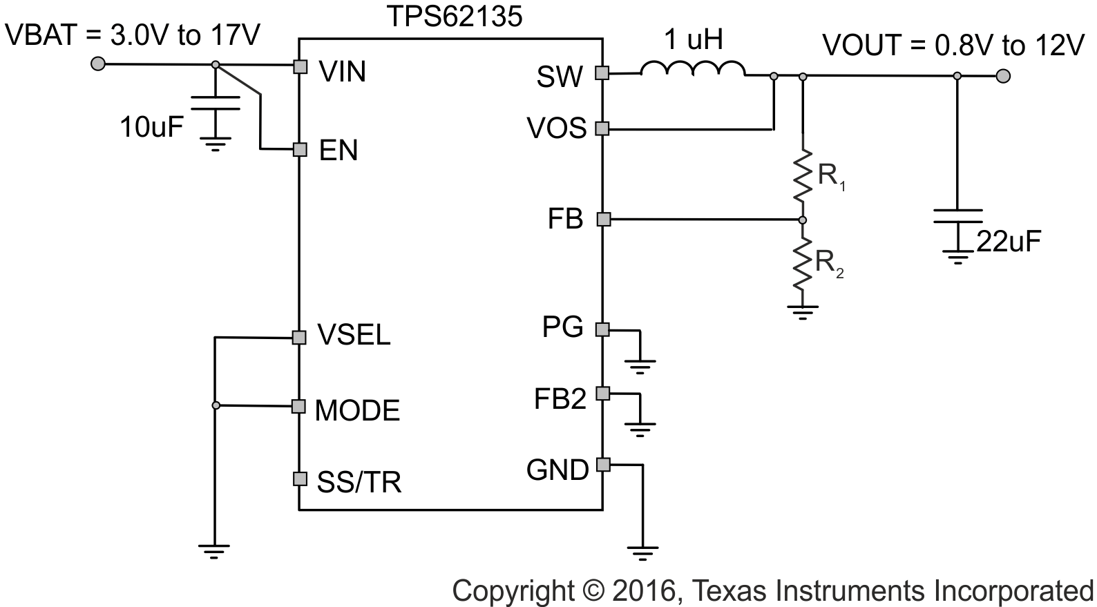
Simplified Schematic

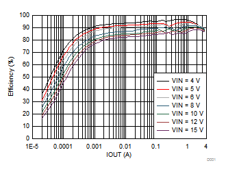
Efficiency vs Output Current for Vo = 3.3 V
