SLVSBH3B June 2016 – April 2017 TPS62135
PRODUCTION DATA.
- 1 Features
- 2 Applications
- 3 Description
- 4 Revision History
- 5 Device Comparison Table
- 6 Pin Configuration and Functions
- 7 Specifications
- 8 Parameter Measurement Information
-
9 Detailed Description
- 9.1 Overview
- 9.2 Functional Block Diagram
- 9.3 Feature Description
- 9.4
Device Functional Modes
- 9.4.1 Pulse Width Modulation (PWM) Operation
- 9.4.2 Power Save Mode Operation (PWM/PFM)
- 9.4.3 100% Duty-Cycle Operation
- 9.4.4 HICCUP Current Limit And Short Circuit Protection (TPS62135 only)
- 9.4.5 Current Limit And Short Circuit Protection (TPS621351 only)
- 9.4.6 Soft-Start / Tracking (SS/TR)
- 9.4.7 Output Discharge Function (TPS62135 only)
- 9.4.8 Starting into a Pre-Biased Load (TPS621351 only)
- 10Application and Implementation
- 11Power Supply Recommendations
- 12Layout
- 13Device and Documentation Support
- 14Mechanical, Packaging, and Orderable Information
Package Options
Mechanical Data (Package|Pins)
- RGX|11
Thermal pad, mechanical data (Package|Pins)
Orderable Information
7 Specifications
7.1 Absolute Maximum Ratings
(1)| MIN | MAX | UNIT | ||
|---|---|---|---|---|
| Pin voltage range(2) | VIN | -0.3 | 20 | V |
| SW, VOS | -0.3 | VIN+0.3 | V | |
| SW (transient for t<10ns)(3) | -2 | 25.5 | V | |
| EN, MODE, VSEL, PG, FB, FB2, SS/TR | -0.3 | VIN+0.3 | V | |
| Operating junction temperature, TJ | -40 | 150 | °C | |
| Storage temperature range, Tstg | -65 | 150 | °C | |
(1) Stresses beyond those listed under Absolute Maximum Ratings may cause permanent damage to the device. These are stress ratings only, which do not imply functional operation of the device at these or any other conditions beyond those indicated under Recommended Operating Conditions. Exposure to absolute-maximum-rated conditions for extended periods may affect device reliability.
(2) All voltages are with respect to network ground pin.
(3) While switching
7.2 ESD Ratings
| VALUE | UNIT | |||
|---|---|---|---|---|
| V(ESD) | Electrostatic discharge | Human Body Model - (HBM), per ANSI/ESDA/JEDEC JS-001(1) | ±2000 | V |
| Charge Device Model - (CDM), per JEDEC specification JESD22-C101(2) | ±500 | V | ||
(1) JEDEC document JEP155 states that 500-V HBM allows safe manufacturing with a standard ESD control process.
(2) JEDEC document JEP157 states that 250-V CDM allows safe manufacturing with a standard ESD control process.
7.3 Recommended Operating Conditions
over operating junction temperature range (unless otherwise noted)| MIN | NOM | MAX | UNIT | |||
|---|---|---|---|---|---|---|
| VIN | Supply voltage range | 3 | 17 | V | ||
| VOUT | Output voltage range | 0.8 | 12 | V | ||
| L | Effective inductance | 0.6 | 1 | 2.9 | µH | |
| CO | Effective output capacitance(1) | 6 | 22 | 200(3) | µF | |
| CI | Effective input capacitance(1)(2) | 3 | 10 | µF | ||
| TJ | Operating junction temperature | -40 | +125 | °C | ||
(1) Due to the dc bias effect of ceramic capacitors, the effective capacitance is lower then the nominal value when a voltage is applied. This is why the capacitance is specified to allow the selection of the smallest capacitor required with the dc bias effect for this type of capacitor in mind. The nominal value given matches a typical capacitor to be chosen to meet the minimum capacitance required.
(2) Larger values may be required if the source impedance can not support the transient requirements of the load.
(3) This is for capacitors directly at the output of the TPS62135x. More capacitance is allowed if there is a series resistance associated to the capacitors. See also the systems examples Powering Multiple Loads for applications where many distributed capacitors are connected to the output.
7.4 Thermal Information
| THERMAL METRIC(1) | TPS62135, TPS621351 | UNIT | |
|---|---|---|---|
| RGX (VQFN) | |||
| 11 PIN | |||
| RθJA | Junction-to-ambient thermal resistance | 38.4 | °C/W |
| RθJC(top) | Junction-to-case (top) thermal resistance | 2.0 | °C/W |
| RθJB | Junction-to-board thermal resistance | 7.6 | °C/W |
| ψJT | Junction-to-top characterization parameter | 0.1 | °C/W |
| ψJB | Junction-to-board characterization parameter | 7.6 | °C/W |
| RθJC(bot) | Junction-to-case (bottom) thermal resistance | 3.2 | °C/W |
(1) For more information about traditional and new thermal metrics, see the Semiconductor and IC Package Thermal Metrics application report. Thermal data is taken according JEDEC 51-5 on a 4-layer pcb with 6 thermal vias.
7.5 Electrical Characteristics
over operating junction temperature (TJ= -40 °C to +125 °C) and VIN= 3 V to 17 V. Typical values at VIN = 12 V and TA= 25 °C. (unless otherwise noted)| PARAMETER | TEST CONDITIONS | MIN | TYP | MAX | UNIT | ||
|---|---|---|---|---|---|---|---|
| SUPPLY | |||||||
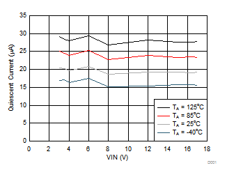
| IQ | Operating Quiescent Current | EN = high, IOUT= 0 mA, Device not switching, TJ= 85 °C | 35 | µA | |||
| IQ | Operating Quiescent Current | EN = high, IOUT= 0 mA, Device not switching | 18 | 46 | µA | ||
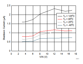
| ISD | Shutdown Current | EN = 0 V, Nominal value at TJ= 25 °C, Max value at TJ= 85 °C | 1 | 8 | µA | ||
| VUVLO | Undervoltage Lockout Threshold | Rising Input Voltage | 2.8 | 2.9 | 3.0 | V | |
| Falling Input Voltage | 2.5 | 2.6 | 2.7 | V | |||
| TSD | Thermal Shutdown Temperature | Rising Junction Temperature | 160 | °C | |||
| Thermal Shutdown Hysteresis | 20 | ||||||
| CONTROL (EN, SS/TR, PG, MODE, VSEL) | |||||||
| VIH | High Level Input Voltage for VSEL, MODE pin | 0.9 | V | ||||
| VIL | Low Level Input Voltage for VSEL, MODE pin | 0.3 | V | ||||
| VIH | Input Threshold Voltage for EN pin; rising edge | 0.77 | 0.8 | 0.83 | V | ||
| VIL | Input Threshold Voltage for EN pin; falling edge | 0.67 | 0.7 | 0.73 | V | ||
| ILKG_EN | Input Leakage Current for EN, VSEL, MODE | VIH = VIN or VIL= GND | 100 | nA | |||
| VTH_PG | Power Good Threshold Voltage; dc level | Rising (%VOUT) | 93% | 96% | 98% | ||
| Hysteresis | Falling (%VOUT) | 3% | 4.5% | ||||
| VOL_PG | Power Good Output Low Voltage | IPG = 2 mA | 0.07 | 0.3 | V | ||
| ILKG_PG | Input Leakage Current (PG) | VPG = 5 V | 100 | nA | |||
| ISS/TR | SS/TR pin source current | 2.5 | µA | ||||
| ISS/TR tolerance | TJ= -40 °C to +125 °C | ±0.2 | µA | ||||
| Tracking gain | VFB / VSS/TR | 1 | |||||
| Tracking offset | feedback voltage with VSS/TR = 0 V | 11 | mV | ||||
| POWER SWITCH | |||||||
| RDS(ON) | High-Side MOSFET ON-Resistance | VIN ≥ 4 V | 100 | 180 | mΩ | ||
| Low-Side MOSFET ON-Resistance | VIN ≥ 4 V | 39 | 67 | mΩ | |||
| ILIMH | High-Side MOSFET Current Limit | dc value(2) | 4.8 | 5.6 | 6.5 | A | |
| ILIML | Low-Side MOSFET Current Limit | dc value(2) | 4.8 | 5.6 | 6.5 | A | |
| ILIMNEG | Negative current limit | dc value | 1.5 | A | |||
| fSW | PWM Switching Frequency | MODE = high; VIN = 12V, VOUT = 3.3V; IOUT = 1A | 2.5 | MHz | |||
| OUTPUT | |||||||
| VFB | Feedback Voltage | 0.7 | V | ||||
| ILKG_FB | Input Leakage Current (FB) | VFB= 0.7 V | 1 | 70 | nA | ||
| VFB | Feedback Voltage Accuracy(1) | VIN ≥ VOUT +1 V | PWM mode | -1% | 1% | ||
| VIN ≥ VOUT +1 V; VOUT ≥ 1.5 V | PFM mode; Co,eff ≥ 47 µF, L = 1 µH | -1% | 2% | ||||
| 1 V ≤ VOUT < 1.5 V | PFM mode; Co,eff ≥ 47 µF, L = 1 µH | -1% | 2.5% | ||||
| VOUT < 1 V | PFM mode; Co,eff ≥ 75 µF, L = 1 µH | -1% | 2.5% | ||||
| VFB | Feedback Voltage Accuracy with Voltage Tracking | VIN ≥ VOUT +1 V; VSS/TR = 0.35 V | PWM mode | -2% | 7.5% | ||
| RDS(ON) | FB2 resistance to GND when VSEL= high | 10 | 30 | Ω | |||
| ILKG_FB2 | Input Leakage Current in FB2 when VSEL = low | 1 | 70 | nA | |||
| Load Regulation | PWM mode operation | 0.05 | %/A | ||||
| Line Regulation | PWM mode operation, IOUT= 1 A, VIN ≥ Vout + 1 V or VIN ≥ 3.5 V whichever is larger | 0.02 | %/V | ||||
| Output Discharge Resistance | TPS62135 only | 100 | Ω | ||||
| tdelay | Start-up Delay time | IO= 0 mA, Time from EN=high to start switching; VIN applied already | 200 | 300 | µs | ||
| tramp | Ramp time; SS/TR pin open | IO= 0 mA, Time from first switching pulse until 95% of nominal output voltage; device not in current limit | 150 | µs | |||
(1) The output voltage accuracy in Power Save Mode can be improved by increasing the output capacitor value, reducing the output voltage ripple (see Pulse Width Modulation (PWM) Operation).
7.6 Typical Characteristics

| EN = low |

| EN = high | device not switching |