SLVSAC5 April 2014 TPS62684
PRODUCTION DATA.
- 1 Features
- 2 Applications
- 3 Description
- 4 Revision History
- 5 Device Comparison Table
- 6 Terminal Configuration and Functions
- 7 Specifications
- 8 Parameter Measurement Information
- 9 Detailed Description
- 10Applications and Implementation
- 11Power Supply Recommendations
- 12Layout
- 13Device and Documentation Support
- 14Mechanical, Packaging, and Orderable Information
Package Options
Mechanical Data (Package|Pins)
- YFF|6
Thermal pad, mechanical data (Package|Pins)
Orderable Information
1 Features
- VIN Range From 3.25V to 5.5V
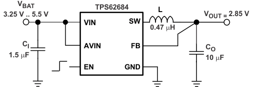
- Total Solution Size <12 mm2
- Three Surface-Mount External Components Required (One 0805 MLCC Inductor, Two small Ceramic Capacitors)
- Complete Sub 1-mm Component Profile Solution
- Spread Spectrum, PWM Frequency Dithering
- Best in Class Load and Line Transient
- ±2% Total DC Voltage Accuracy
- Up to 1600mA load current
- 5.5MHz Regulated Frequency Operation
- Available in a 6-Pin NanoFree™ (WCSP)
2 Applications
- Tablet PC
- Cell Phones, Smart-Phones
- Digital TV, WLAN, GPS and Bluetooth® Applications
3 Description
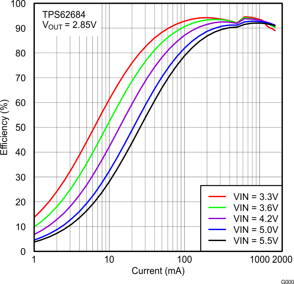
The TPS62684 is a high-frequency synchronous step-down dc-dc converter optimized for battery-powered portable applications in which high load currents in a very small solution size and height are required. The TPS62684 is optimized for high efficiency and low output voltage ripple, supports up to 1600-mA load current and allows the use of low cost chip inductor and capacitors. With a input voltage range of 3.25V to 5.5V, the device supports applications powered by Li-Ion batteries as well as 5V rails.
The TPS62684 operates at a 5.5-MHz switching frequency with PWM spread spectrum capability. For noise-sensitive applications, this provides a lower noise regulated output, as well as low noise at the input. The device supports a 2.85V fixed output voltage, requiring no external feedback network.
These features, combined with high PSRR and AC load regulation performance, make this device suitable to replace a linear regulator to obtain better power conversion efficiency.
Device Information
| ORDER NUMBER | PACKAGE | BODY SIZE |
|---|---|---|
| TPS62684YFF | DSBGA (6) | 1.431mm × 1.135mm |
Smallest Solution Size Application
Efficiency vs Load Current