SLVSAC5 April 2014 TPS62684
PRODUCTION DATA.
- 1 Features
- 2 Applications
- 3 Description
- 4 Revision History
- 5 Device Comparison Table
- 6 Terminal Configuration and Functions
- 7 Specifications
- 8 Parameter Measurement Information
- 9 Detailed Description
- 10Applications and Implementation
- 11Power Supply Recommendations
- 12Layout
- 13Device and Documentation Support
- 14Mechanical, Packaging, and Orderable Information
Package Options
Mechanical Data (Package|Pins)
- YFF|6
Thermal pad, mechanical data (Package|Pins)
Orderable Information
10 Applications and Implementation
10.1 Application Information
10.1.1 Inductor Selection
The TPS62684 series of step-down converters have been optimized to operate with an effective inductance value in the range of 0.3μH to 1.2μH and with output capacitors in the range of 3μF up to 30μF effective capacitance. The internal compensation is optimized to operate with an output filter of Lnominal = 0.47μH or 0.56μH and CO_effective = 5μF. Larger or smaller inductor values can be used to optimize the performance of the device for specific operation conditions. For more details, see the CHECKING LOOP STABILITY section.
The inductor value affects its peak-to-peak ripple current, the output voltage ripple and the efficiency. The selected inductor has to be rated for its dc resistance and saturation current. The inductor ripple current (ΔIL) decreases with higher inductance and increases with higher VIN or VOUT.
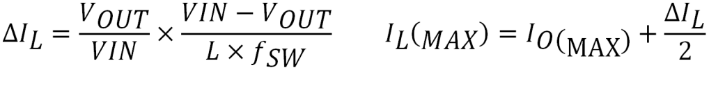
where
In high-frequency converter applications, the efficiency is primarily affected by the inductor AC resistance (i.e. quality factor) and to a smaller extent by the inductor DCR value. To achieve high efficiency operation, care should be taken in selecting inductors featuring a quality factor above 25 at the switching frequency. Increasing the inductor value produces lower RMS currents, but degrades transient response. For a given physical inductor size, increased inductance usually results in an inductor with lower saturation current.
The total inductor losses consist of both the losses in the DC resistance (DCR) and the following frequency-dependent components:
- The losses in the core material (magnetic hysteresis loss, especially at high switching frequencies)
- Additional losses in the conductor from the skin effect (current displacement at high frequencies)
- Magnetic field losses of the neighboring windings (proximity effect)
- Radiation losses
For smallest solution size a 0805 size (2mm x 1.2mm) chip inductor can be used. Please note that the DC resistance of the inductor is directly related to its volume (LxWxH). Therefore designing for smallest solution size negatively impacts the overall efficiency at heavy load currents.
The following inductor series from different suppliers have been used with the TPS62684 converter.
Table 1. List Of Inductors(1)
| MANUFACTURER | SERIES | DIMENSIONS (in mm) |
|---|---|---|
| TOKO | MDT2012-CRR56N | 2.0 x 1.2 x 1.0 max. height |
| DFE252012P-R47(2) | 2.5 x 2.0 x 1.2 max. height | |
| MURATA | LQM21PNR47MGO | 2.0 x 1.2 x 1.0 max. height |
| LQM2MPNR47MGH | 2.0 x 1.6 x 1.0 max. height |
10.1.2 Output Capacitor Selection
The advanced fast-response voltage mode control scheme of the TPS62684 allows the use of tiny ceramic capacitors. Ceramic capacitors with low ESR values have the lowest output voltage ripple and are recommended. For best performance, the device should be operated with a minimum effective output capacitance of 5μF. A total effective output capacitance between 3μF and 30μF is required. The output capacitor requires either an X7R or X5R dielectric. Y5V and Z5U dielectric capacitors, aside from their wide variation in capacitance over temperature, become resistive at high frequencies.
The device operates in PWM mode and the overall output voltage ripple is the sum of the voltage step caused by the output capacitor ESL and the ripple current flowing through the output capacitor impedance.
10.1.3 Output Filter Design
The inductor and the output capacitor build the output filter. As recommended in the output capacitor and inductor sections, these components should be in the range:
- CO = 3µF to 30µF (total effective capacitance)
- L = 0.3 µH to 1.2 µH (effective inductance)
For best transient performance, the internal control stage is optimized for a LCO product of 0.5µH x 10µF (nominal values).
10.1.4 Input Capacitor Selection
Because the nature of the buck converter has a pulsating input current, a low ESR input capacitor is required to prevent large voltage transients that cause misbehavior of the device or interferences with other circuits in the system. For most applications, a 1.5-μF nominal capacitor (≥ 0.5μF effective capacitance) with a X5R or X7R dielectric is sufficient. If the application exhibits a noisy or erratic switching frequency, the remedy is likely found by increasing the value of the input capacitor.
Take care when using only ceramic input capacitors. When a ceramic capacitor is used at the input and the power is being supplied through long wires, such as from a wall adapter, a load step at the output can induce ringing at the VIN pin. This ringing can couple to the output and be mistaken as loop instability or could even damage the part. Additional "bulk" capacitance (electrolytic or tantalum) should in this circumstance be placed between CI and the power source lead to reduce ringing than occurs between the inductance of the power source leads and CI.
10.1.5 Checking Loop Stability
The first step of circuit and stability evaluation is to look, from a steady-state perspective, at the following signals:
- Switching node, SW
- Inductor current, IL
- Output ripple voltage, VOUT(AC)
These are the basic signals that need to be measured when evaluating a switching converter. When the switching waveform shows large duty cycle jitter or the output voltage or inductor current shows oscillations, the regulation loop may be unstable. This is typically caused by board layout and/or LCO combination.
As a next step in the evaluation of the regulation loop, the load transient response is tested. The time between the application of the load transient and the turn on of the high side MOSFET, the output capacitor supplies all of the current required by the load. VOUT immediately shifts by an amount equal to ΔI(LOAD) x ESR, where ESR is the effective series resistance of CO. ΔI(LOAD) begins to charge or discharge CO generating a feedback error signal used by the regulator to return VOUT to its steady-state value.
During this recovery time, VOUT can be monitored for settling time, overshoot or ringing that helps judge the converter’s stability. Without any ringing, the loop usually has more than 45° of phase margin.
Because the damping factor of the circuitry is directly related to several resistive parameters (e.g., MOSFET RDS(on)) that are temperature dependent, the loop stability analysis should be done over the input voltage range, load current range, and temperature range.
10.2 Typical Application
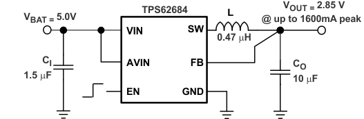 Figure 26. Typical Application Circuit
10.2.1 Design Requirements
Figure 26 shows the schematic of the typical application. The TPS62684 allows the design of a power supply with small solution size. In order to properly dissipate the heat, wide copper traces for the power connections should be used to distribute the heat across the PCB. If possible, a GND plane should be used as it provides a low impedance connection as well as serves as a heat sink. The EN pin should be set high after the supply voltage has ramped to at least the minimum input voltage level of 3.25V.
10.2.2 Detailed Design Procedure
The TPS62684 allows the design of a complete power supply with only 3 small external components. A X5R or X7R ceramic input capacitor close to the VIN pin and GND pin with a nominal value of 1.5uF or higher is required. The input capacitance can be increased in case the source impedance is large or if there are high load transients expected at the output. The inductor should be placed close to the SW node with a saturation current above the current limit. A X5R or X7R ceramic output capacitor should be placed close to the inductor terminal and GND. A low impedance GND connection on the output capacitor is required. The feedback (FB) pin should be routed to the terminal of the output capacitor. The dc bias effect of the input and output capacitors must be taken into account and the total capacitance on the output must not exceed the value given in the recommended operating conditions.
10.2.3 Application Curves
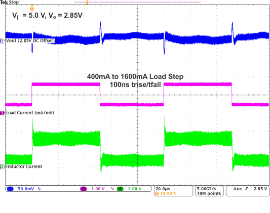 Figure 27. Load Transient Response
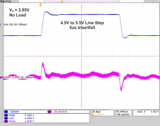 Figure 28. Line Transient Response