SLVSAC5 April 2014 TPS62684
PRODUCTION DATA.
- 1 Features
- 2 Applications
- 3 Description
- 4 Revision History
- 5 Device Comparison Table
- 6 Terminal Configuration and Functions
- 7 Specifications
- 8 Parameter Measurement Information
- 9 Detailed Description
- 10Applications and Implementation
- 11Power Supply Recommendations
- 12Layout
- 13Device and Documentation Support
- 14Mechanical, Packaging, and Orderable Information
Package Options
Mechanical Data (Package|Pins)
- YFF|6
Thermal pad, mechanical data (Package|Pins)
Orderable Information
9 Detailed Description
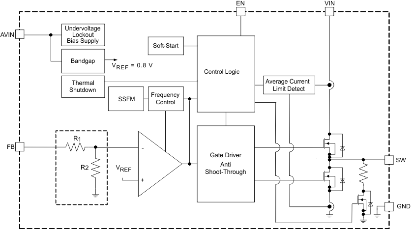
9.1 Overview
9.1.1 Operation
The TPS62684 is a synchronous step-down converter typically operating at a regulated 5.5-MHz pulse width modulation (PWM) frequency.
The converter uses a unique frequency locked ring oscillating modulator to achieve best-in-class load and line response which allows the use of tiny inductors and small ceramic input and output capacitors. At the beginning of each switching cycle, the N-channel high side MOSFET switch is turned on and the inductor current ramps up. This raises the output voltage until the main comparator trips; then the control logic turns off the switch.
One key advantage of the non-linear architecture that there is no traditional feedback loop. The loop response time to a change in VOUT is essentially instantaneous. The absence of a traditional, high-gain compensated linear loop means that the TPS62684 is inherently stable over a range of L and CO.
9.1.2 Switching Frequency
When high or low duty cycles are encountered, the loop runs out of range and the conversion frequency falls below 5.5MHz. The tendency is for the converter to operate more towards a "constant inductor peak current" rather than a "constant frequency". In addition to this behavior which is observed at high duty cycles, it is also noted at low duty cycles.
When the converter is required to operate towards the 5.5MHz nominal at extreme duty cycles, the application is assisted by decreasing the ratio of inductance (L) to the output capacitor's equivalent series inductance (ESL). This increases the ESL step seen at the FB pin input, decreasing the propagation delay which increases the switching frequency.
9.2 Functional Block Diagram
9.3 Feature Description
9.3.1 Spread Spectrum, PWM Frequency Dithering
The goal is to spread out the emitted RF energy over a larger frequency range, so that the resulting EMI is similar to white noise. The end result is a spectrum that is continuous and lower in peak amplitude, making it easier to comply with electromagnetic interference (EMI) standards and with power supply ripple requirements in cellular and non-cellular wireless applications. Radio receivers are typically susceptible to narrowband noise that is focused on specific frequencies.
Switching regulators can be particularly troublesome in applications where electromagnetic interference (EMI) is a concern. Switching regulators operate on a cycle-by-cycle basis to transfer power to their output. In most cases, the frequency of operation is either fixed or regulated, based on the output load. This method of conversion creates large components of noise at the frequency of operation (fundamental) and multiples of the operating frequency (harmonics).
The spread spectrum architecture varies the switching frequency by around ±10% of the nominal switching frequency, thereby significantly reducing the peak radiated and conducted noise on both the input and output supplies. The frequency dithering scheme is modulated with a triangle profile and a modulation frequency fm.
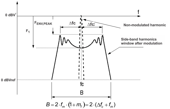 Figure 24. Spectrum Of A Frequency Modulated Sin. Wave With Sinusoidal Variation In Time
 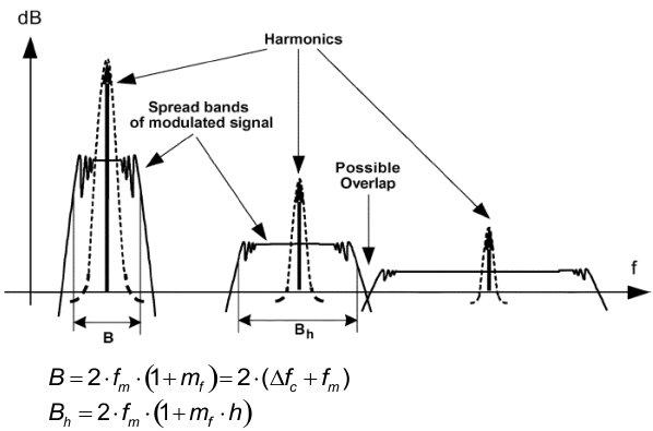 Figure 25. Spread Bands Of Harmonics In Modulated Square Signals
 The above figures show that after modulation the side-band harmonic is attenuated compared to the non-modulated harmonic, and the harmonic energy is spread into a certain frequency band. The higher the modulation index (mf), the larger the attenuation.
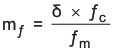
where:
fc is the carrier frequency (5.5MHz)
fm is the modulating frequency (approx. 0.008*fc)
δ is the modulation ratio (approx 0.1)

The maximum switching frequency fc is limited by the device and finally the parameter modulation ratio (δ), together with fm, which is the side-band harmonic´s bandwidth around the carrier frequency fc. The bandwidth of a frequency modulated waveform is approximately given by Carson’s rule and is summarized as:

fm < RBW (resolution bandwidth): The receiver is not able to distinguish individual side-band harmonics, so, several harmonics are added in the input filter and the measured value is higher than expected in theoretical calculations.
fm > RBW: The receiver is able to properly measure each individual side-band harmonic separately, so the measurements match with the theoretical calculations.
9.4 Device Functional Modes
9.4.1 Enable
The TPS62684 device starts operation when EN is set high. For proper operation, the EN pin must be terminated and must not be left floating. The device should only be enabled when the input voltage is stable and has ramped above its minimum supply of 3.25V.
Pulling the EN pin low forces the device into shutdown, with a shutdown current of typically 0.2μA. In this mode, the internal high side and low side MOSFETs are turned off, the internal resistor feedback divider is disconnected, and the entire internal-control circuitry is switched off. The TPS62684 device actively discharges the output capacitor when it turns off. The integrated discharge resistor has a typical resistance of 12Ω. This internal discharge transistor is only turned on after the device had been enabled at least once. The required time to discharge the output capacitor at the output node depends on load current and the effective output capacitance. The TPS62684 is designed such that it can start into a pre-biased output, in case the output discharge circuit was active for too short a time to fully discharge the output capacitor. In this case, the converter starts switching as soon as the internal reference has approximately reached the equivalent voltage to the output voltage present. It then ramps the output from that voltage level to its target value.
9.4.2 Soft Start
The TPS62684 has an internal soft start circuit that controls the ramp up of the output voltage. Once the converter is enabled and the input voltage is above the undervoltage lockout threshold VUVLO, the output voltage ramps up to 95% of its nominal value within tRamp of typ. 150μs. This ensures a controlled ramp up of the output voltage and limits the input voltage drop when a battery or a high-impedance power source is connected to the input of the DC/DC converter.
The inrush current during start-up is directly related to the effective capacitance and load present at the output of the converter.
During soft start, the current limit is reduced to 2/3 of its nominal value. Once the internal reference voltage has reached 90% of its target value, the current limit is set to its nominal target value.
9.4.3 Undervoltage Lockout
The undervoltage lockout circuit prevents the device from misoperation at low input voltages. It prevents the converter from turning on either MOSFET under undefined conditions. The TPS62684 has a rising UVLO threshold of 2.1V (typical).
9.4.4 Short-Circuit Protection
The TPS62684 integrates current limit circuitry to protect the device against heavy load or short circuits. When the average current in the high side MOSFET reaches its current limit, the high side MOSFET is turned off and the low side MOSFET is turned on ramping down the inductor current.
As soon as the converter detects a short circuit condition it shuts down. After a delay of approximately 20 µs, the converter restarts. In case the short circuit condition remains, the converter shuts down again after hitting the current limit threshold. In case the short circuit condition remains present on the converters output, the converter periodically re-starts with a small duty cycle as the output voltage is zero and shuts down again, thereby limiting the current drawn from the input.
9.4.5 Thermal Shutdown
As soon as the junction temperature, TJ, exceeds typically 140°C, the device goes into thermal shutdown. In this mode, the power stage is turned off. The device continues its operation when the junction temperature falls below typically 130°C.