SLVSAC5 April 2014 TPS62684
PRODUCTION DATA.
- 1 Features
- 2 Applications
- 3 Description
- 4 Revision History
- 5 Device Comparison Table
- 6 Terminal Configuration and Functions
- 7 Specifications
- 8 Parameter Measurement Information
- 9 Detailed Description
- 10Applications and Implementation
- 11Power Supply Recommendations
- 12Layout
- 13Device and Documentation Support
- 14Mechanical, Packaging, and Orderable Information
Package Options
Mechanical Data (Package|Pins)
- YFF|6
Thermal pad, mechanical data (Package|Pins)
Orderable Information
7 Specifications
7.1 Absolute Maximum Ratings
over operating free-air temperature range (unless otherwise noted)(1)| MIN | MAX | UNIT | ||
|---|---|---|---|---|
| VI | Voltage at VIN(2) | –0.3 | 6 | V |
| Voltage at FB(2) | –0.3 | 3.6 | ||
| Voltage at SW, EN, AVIN (2) | –0.3 | VIN + 0.3 | ||
| Continuous average output current(4) | 890 | mA | ||
| Peak output current(4) | 1600 | mA | ||
| TJ | Operating junction temperature(3) | -40 | 150 | °C |
(1) Stresses beyond those listed under absolute maximum ratings may cause permanent damage to the device. These are stress ratings only and functional operation of the device at these or any other conditions beyond those indicated under recommended operating conditions is not implied. Exposure to absolute-maximum-rated conditions for extended periods may affect device reliability.
(2) All voltage values are with respect to network ground terminal.
(3) In applications where high power dissipation and/or poor package thermal resistance is present, the maximum ambient temperature may have to be derated. Maximum ambient temperature (TA(max)) is dependent on the maximum operating junction temperature (TJ(max)), the maximum power dissipation of the device in the application (PD(max)), and the junction-to-ambient thermal resistance of the part/package in the application (θJA), as given by the following equation: TA(max)= TJ(max)–(θJA X PD(max)). To achieve full lifetime, it is recommended to operate the device with a maximum junction temperature of 105°C.
(4) Limit the junction temperature to 105°C.
7.2 Handling Ratings
| MIN | MAX | UNIT | ||
|---|---|---|---|---|
| Tstg | Storage temperature range | –65 | 150 | °C |
| ESD rating (1) | Human body model | 2 | kV | |
| Charge device model | 1 | |||
| Machine model | 100 | V |
(1) The human body model is a 100-pF capacitor discharged through a 1.5-kΩ resistor into each pin. The machine model is a 200-pF capacitor discharged directly into each pin.
7.3 Recommended Operating Conditions
| MIN | NOM | MAX | UNIT | ||||
|---|---|---|---|---|---|---|---|
| VIN | Input voltage range | 3.25 | 5.5 | V | |||
| IO | Peak output current(1) | VIN < VOUT,nom + 1V | 0 | 960 | mA | ||
| VOUT,nom + 1V ≤ VIN ≤ 5.5V | 0 | 1600 | |||||
| CI | Effective Input Capacitance(2)(3) | 0.5 | µF | ||||
| L | Effective Inductance | 0.3 | 1.2 | µH | |||
| CO | Effective Output Capacitance(2) | 3.0 | 5.0 | 30 | µF | ||
| TA | Ambient temperature(4) | –40 | +85 | °C | |||
| TJ | Operating junction temperature(5) | –40 | +125 | °C | |||
(1) Operating beyond the continuous average output current of 890mA may decrease the lifetime. See the Thermal, Lifetime Information and Maximum Output Current section.
(2) Due to the dc bias effect of ceramic capacitors, the effective capacitance is lower than the nominal value when a voltage is applied. The capacitance is specified to allow the selection of the appropriate capacitor taking into account its dc bias effect.
(3) Larger values may be required if the source impedance can not support the transient requirements of the load.
(4) In applications where high power dissipation and/or poor package thermal resistance is present, the maximum ambient temperature may have to be derated. Maximum ambient temperature (TA(max)) is dependent on the maximum operating junction temperature (TJ(max)), the maximum power dissipation of the device in the application (PD(max)), and the junction-to-ambient thermal resistance of the part/package in the application (θJA), as given by the following equation: TA(max)= TJ(max)–(θJA X PD(max)). To achieve full lifetime, it is recommended to operate the device with a maximum junction temperature of 105°C.
(5) Limit the junction temperature to 105°C at 1.6A output current for a lifetime of 25k hours.
7.4 Thermal Information
| THERMAL METRIC(1) | TPS62684 | UNIT | |
|---|---|---|---|
| YFF | |||
| 6 TERMINALS | |||
| RθJA | Junction-to-ambient thermal resistance | 108.9 | °C/W |
| RθJC(top) | Junction-to-case (top) thermal resistance | 1.0 | |
| RθJB | Junction-to-board thermal resistance | 17.5 | |
| ψJT | Junction-to-top characterization parameter | 4.1 | |
| ψJB | Junction-to-board characterization parameter | 17.5 | |
| RθJC(bot) | Junction-to-case (bottom) thermal resistance | n/a | |
(1) For more information about traditional and new thermal metrics, see the IC Package Thermal Metrics application report, SPRA953.
7.5 Electrical Characteristics
Minimum and maximum values are at VI = 3.25V to 5.5V, EN = VIN and TA = –40°C to 85°C; Circuit of Parameter Measurement Information section (unless otherwise noted). Typical values are at VIN = 3.6V, EN = VIN and TA = 25°C (unless otherwise noted).| PARAMETER | TEST CONDITIONS | MIN | TYP | MAX | UNIT | |||
|---|---|---|---|---|---|---|---|---|
| SUPPLY CURRENT into VIN + AVIN | ||||||||
| IQ | Operating quiescent current | IO = 0mA | 5.8 | mA | ||||
| ISD | Shutdown current | EN = low; not including high side MOSFET leakage |
0.2 | 1.5 | μA | |||
| VUVLO | Undervoltage lockout threshold | VIN rising | 2.1 | 2.3 | V | |||
| VIN falling | 1.95 | 2.1 | V | |||||
| ENABLE | ||||||||
| VIH | High-level input voltage | 0.9 | V | |||||
| VIL | Low-level input voltage | 0.4 | V | |||||
| Ilkg,EN | Input leakage current | EN connected to GND or VIN; TJ = –40°C to 85°C | 0.01 | 0.1 | μA | |||
| POWER SWITCH | ||||||||
| RDS(on),HS | High Side MOSFET on resistance | VIN = 3.6V; TJ = –40°C to 125°C | 95 | 155 | mΩ | |||
| VIN = 2.5V | 170 | mΩ | ||||||
| Ilkg,HS | High Side MOSFET leakage current | VIN = 5.5V; TJ = –40°C to 85°C | 2.6 | μA | ||||
| RDS(on),LS | Low Side MOSFET on resistance | VIN = 3.6V; TJ = –40°C to 125°C | 75 | 155 | mΩ | |||
| VIN = 2.5V | 100 | mΩ | ||||||
| Ilkg,LS | Low Side MOSFET leakage current | VIN = 5.5V; TJ = –40°C to 85°C | 1 | μA | ||||
| Resistor in parallel to Low Side MOSFET | 250 | kΩ | ||||||
| RDIS | Discharge resistor for power-down sequence | only active after a first power-up (EN = high to low after VIN applied) | 12 | Ω | ||||
| Average High Side MOSFET current limit | 1680 | 2100 | 2850 | mA | ||||
| Input current limit under short-circuit conditions | VOUT shorted to ground | 150 | mA | |||||
| Thermal shutdown | Temperature rising | 140 | °C | |||||
| Thermal shutdown hysteresis | Temperature falling | 10 | °C | |||||
| OSCILLATOR | ||||||||
| fSW | Nominal oscillator frequency | IOUT = 0mA | 5.5 | MHz | ||||
| OUTPUT | ||||||||
| VOUT,nom | Nominal output voltage | 2.85 | V | |||||
| Output voltage accuracy | 3.25V ≤ VIN ≤ 3.85V, 0mA ≤ IO ≤ 960 mA | 0.98×VOUT,NOM | VOUT,NOM | 1.02×VOUT,NOM | V | |||
| 3.85V ≤ VIN ≤ 5.5V, 0mA ≤ IO ≤ 1600 mA | 0.98×VOUT,NOM | VOUT,NOM | 1.02×VOUT,NOM | V | ||||
| Line regulation | VIN = VOUT + 0.5V (min 3.25V) to 5.5V, IO = 200 mA | 0.2 | %/V | |||||
| Load regulation | IO = 0mA to 1600 mA | –0.00085 | %/mA | |||||
| FB pin input resistance | 1.4 | MΩ | ||||||
7.6 Timing Requirements
| MIN | TYP | MAX | UNIT | |||
|---|---|---|---|---|---|---|
| Start-up delay time | IO = 0mA, Time from EN = high to start switching | 120 | 300 | µs | ||
| tRAMP | ramp time | IO = 0mA, Time from start switching until 95% of nominal output voltage | 150 | µs | ||
| Shutdown time | IO = 0mA, Time from EN = low to VO < 500mV, Effective Output Capacitance CO_effective = 5µF | 300 | µs | |||
7.7 Typical Characteristics
| TABLE OF GRAPHS | FIGURE | ||
|---|---|---|---|
| η | Efficiency | vs Load current | Figure 1, Figure 2, Figure 3, Figure 4 |
| vs Input voltage | Figure 5 | ||
| Load transient response | Figure 8, Figure 9, Figure 10, Figure 11, Figure 12, Figure 13, Figure 14 | ||
| AC load transient response | Figure 15 | ||
| Line Transient Response | Figure 16 | ||
| VOUT | DC output voltage | vs Load current | Figure 6, Figure 7 |
| fsw | PWM switching frequency | vs Input voltage | Figure 17 |
| PWM switching frequency | vs Load Current | Figure 18 | |
| PWM operation | Figure 19 | ||
| Spread spectrum frequency modulation operation | Figure 20 | ||
| Start-up | Figure 21, Figure 22 | ||
| Shutdown | Figure 23 | ||
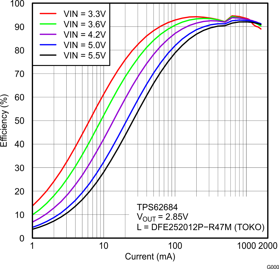 Figure 1. Efficiency Vs Load Current
 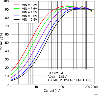 Figure 2. Efficiency Vs Load Current
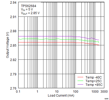
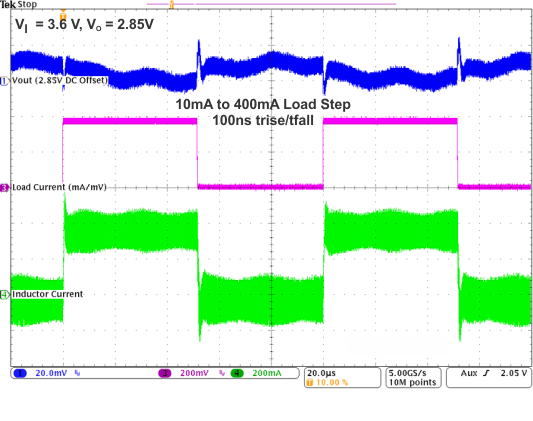 Figure 9. Load Transient Response
 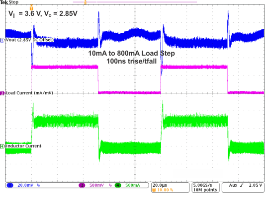 Figure 11. Load Transient Response
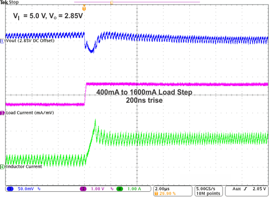
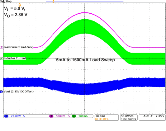 Figure 15. AC Load Transient Response
 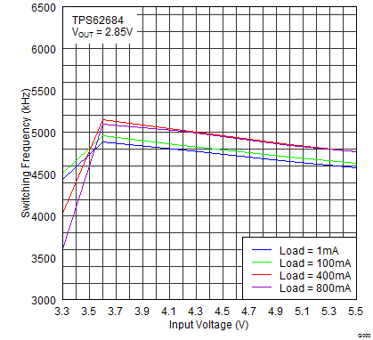 Figure 17. PWM Switching Frequency Vs Input Voltage
 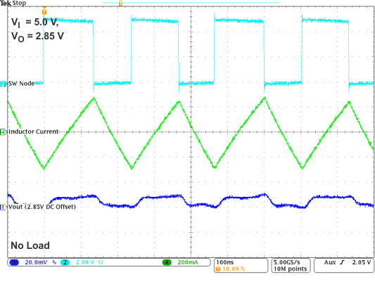 Figure 19. PWM Operation
 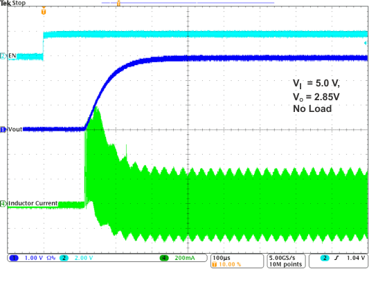 Figure 21. Start-Up
 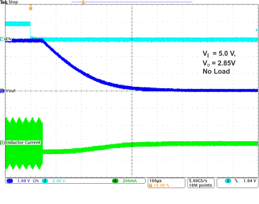 Figure 23. Shutdown
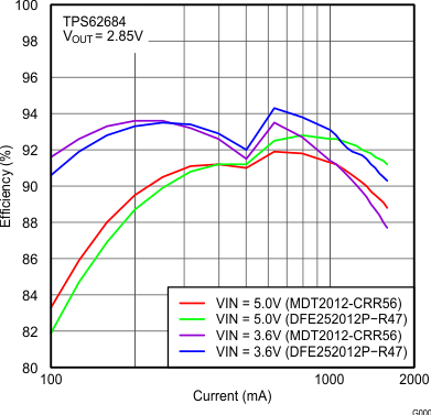
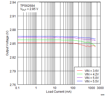
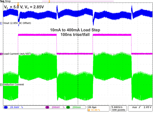
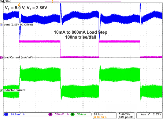 Figure 10. Load Transient Response
 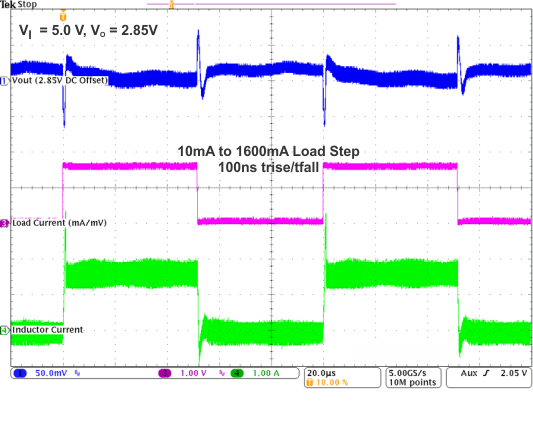 Figure 12. Load Transient Response
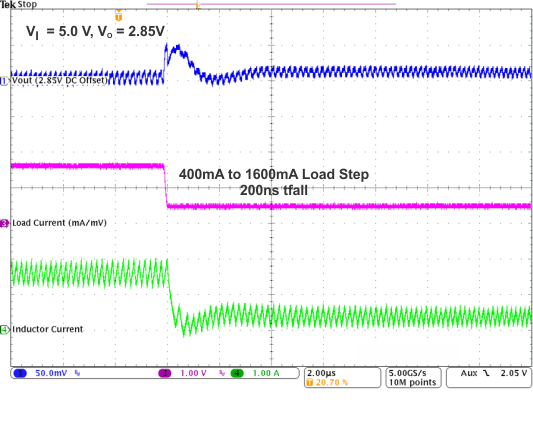
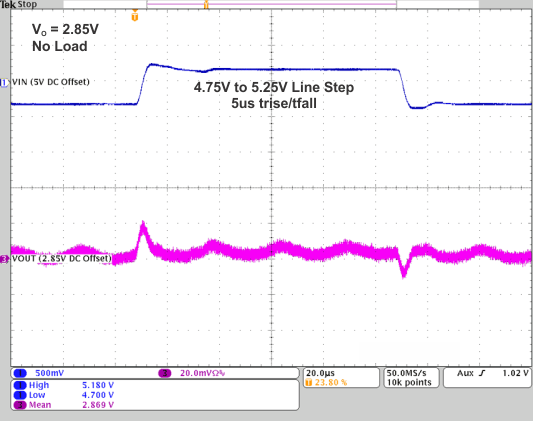 Figure 16. Line Transient Response
 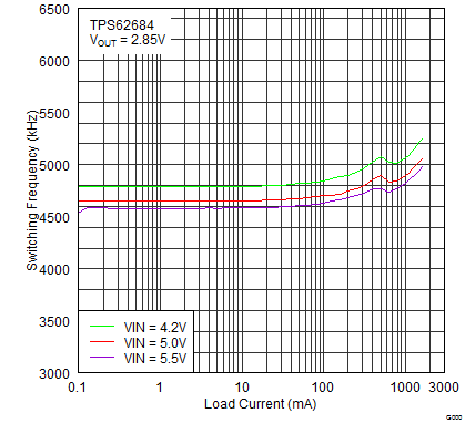 Figure 18. PWM Switching Frequency Vs Load Current
 Figure 20. Spread Spectrum Frequency Modulation Operation
 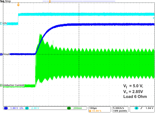 Figure 22. Start-Up