SLVSAC5 April 2014 TPS62684
PRODUCTION DATA.
- 1 Features
- 2 Applications
- 3 Description
- 4 Revision History
- 5 Device Comparison Table
- 6 Terminal Configuration and Functions
- 7 Specifications
- 8 Parameter Measurement Information
- 9 Detailed Description
- 10Applications and Implementation
- 11Power Supply Recommendations
- 12Layout
- 13Device and Documentation Support
- 14Mechanical, Packaging, and Orderable Information
Package Options
Mechanical Data (Package|Pins)
- YFF|6
Thermal pad, mechanical data (Package|Pins)
Orderable Information
12 Layout
12.1 Layout Guidelines
As for all switching power supplies, the layout is an important step in the design. High-speed operation of the TPS62684 demands careful attention to PCB layout. Care must be taken in board layout to get the specified performance. If the layout is not carefully done, the regulator could show poor line and/or load regulation, stability and switching frequency issues as well as EMI problems. It is critical to provide a low inductance, low impedance ground path. Therefore, use wide and short traces for the main current paths.
The input capacitor as well as the inductor and output capacitor should be placed as close as possible to the IC pins. The feedback line should be routed away from noisy components and traces (e.g. SW line).
Figure 29 shows the recommended layout using a 0805 (2.0 mm x 1.2 mm) chip inductor, a 0402 input capacitor and a 0603 output capacitor. Total solution size is 12mm².
12.2 Layout Example
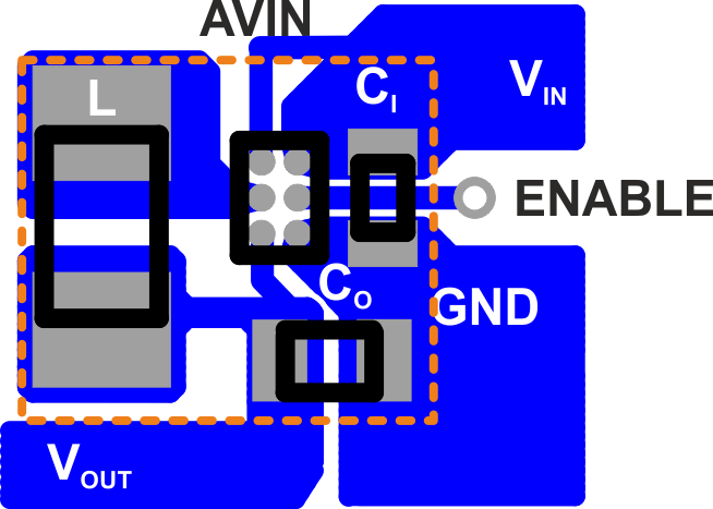 Figure 29. Suggested Layout (Top)
12.3 Thermal, Lifetime Information and Maximum Output Current
Implementation of integrated circuits in wafer chipscale packages requires special attention to power dissipation. Many system-dependent issues such as thermal coupling, airflow, added heat sinks, and convection surfaces, and the presence of other heat-generating components, affect the power-dissipation limits of a given component.
Three basic approaches for enhancing thermal performance are listed below:
- Improving the power dissipation capability of the PCB design
- Improving the thermal coupling of the component to the PCB
- Introducing airflow into the system
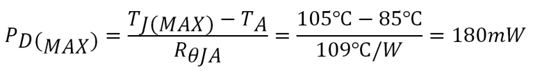
The maximum recommended junction temperature (TJ) of the TPS62684 for full 100k hour lifetime is 105°C. The thermal resistance of the 6-pin WCSP package (YFF-6) is RθJA = 108.9°C/W. Regulator operation is specified to a maximum steady-state ambient temperature TA of 85°C. Therefore, the maximum power dissipation at TJ=105°C is about 180 mW and at TJ=125°C is about 367mW.
Proper PCB layout with a focus on thermal performance results in a reduced junction-to-ambient thermal resistance RθJA and thereby reduces the device junction temperature, TJ.
The maximum peak output current of 1600mA for TPS62684 is defined by its internal current limit. The maximum dc output current over lifetime (100k hours at TJ= 105°C) is 890mA. The device can supply peak output currents above 890mA, so long as there are corresponding output currents below 890mA such that the average output current remains below 890mA, while keeping the junction temperature below 105°C. Operating at output currents above 890mA at junction temperatures above 105°C reduces the lifetime by electromigration effects.
For output currents above 960mA, a minimum supply voltage of 3.85V is recommended.