SLUSDM1A March 2020 – December 2021 TPS62816-Q1
PRODUCTION DATA
- 1 Features
- 2 Applications
- 3 Description
- 4 Revision History
- 5 Device Comparison Table
- 6 Pin Configuration and Functions
- 7 Specifications
- 8 Parameter Measurement Information
- 9 Detailed Description
- 10Application and Implementation
- 11Power Supply Recommendations
- 12Layout
- 13Device and Documentation Support
- 14Mechanical, Packaging, and Orderable Information
Package Options
Mechanical Data (Package|Pins)
- RWY|9
Thermal pad, mechanical data (Package|Pins)
- RWY|9
Orderable Information
10.2.2 Detailed Design Procedure
Equation 10. 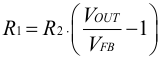
With VFB = 0.6 V:
Table 10-2 Setting the Output Voltage
| NOMINAL OUTPUT VOLTAGE VOUT | R1 | R2 | CFF | EXACT OUTPUT VOLTAGE |
|---|---|---|---|---|
| 0.8 V | 16.9 kΩ | 51 kΩ | 15 pF | 0.7988 V |
| 1.0 V | 20 kΩ | 30 kΩ | 13 pF | 1.0 V |
| 1.1 V | 39.2 kΩ | 47 kΩ | 6.8 pF | 1.101 V |
| 1.2 V | 68 kΩ | 68 kΩ | 3.9 pF | 1.2 V |
| 1.5 V | 76.8 kΩ | 51 kΩ | 3.3 pF | 1.5 V |
| 1.8 V | 80.6 kΩ | 40.2 kΩ | 3.3 pF | 1.803 V |
| 2.5 V | 47.5 kΩ | 15 kΩ | 5.6 pF | 2.5 V |
| 3.3 V | 88.7 kΩ | 19.6 kΩ | 3 pF | 3.315 V |
The maximum value for the feedforward capacitor CFF at minimum output capacitance is determined by Equation 11:
Equation 11. CFF,max(F) = 2.661 ×
10-7 F × Ω / R1 (Ω)