SLUSDU8F September 2019 – October 2023 TPS62860 , TPS62861
PRODUCTION DATA
- 1
- 1 Features
- 2 Applications
- 3 Description
- 4 Revision History
- 5 Device Comparison Table
- 6 Pin Configuration and Functions
- 7 Specifications
-
8 Detailed Description
- 8.1 Overview
- 8.2 Functional Block Diagram
- 8.3
Feature Description
- 8.3.1 Power Save Mode
- 8.3.2 Forced PWM Operation
- 8.3.3 Smart Enable and Shutdown (EN)
- 8.3.4 Soft Start
- 8.3.5 Output Voltage Selection (VSEL) for TPS62860x
- 8.3.6 Output Voltage Selection (VSEL and I2C)
- 8.3.7 Forced PWM Mode During Output Voltage Change
- 8.3.8 Undervoltage Lockout (UVLO)
- 8.3.9 Power Good (PG)
- 8.3.10 Switch Current Limit and Short Circuit Protection
- 8.3.11 Thermal Shutdown
- 8.3.12 Output Voltage Discharge
- 8.4 Programming
- 8.5 Register Map
- 9 Application and Implementation
- 10Device and Documentation Support
- 11Mechanical, Packaging, and Orderable Information
Package Options
Mechanical Data (Package|Pins)
- YCH|8
Thermal pad, mechanical data (Package|Pins)
Orderable Information
9.2.2.1 Inductor Selection
The inductor value affects the peak-to-peak ripple current, the PWM-to-PFM transition point, the output voltage ripple, and the efficiency. The selected inductor has to be rated for its DC resistance and saturation current. The inductor ripple current (ΔIL) decreases with higher inductance and increases with higher VIN or VOUT and can be estimated according to Equation 1.
Equation 2 calculates the maximum inductor current under static load conditions. The saturation current of the inductor must be rated higher than the maximum inductor current, as calculated with Equation 2. This is recommended because during a heavy load transient the inductor current rises above the calculated value. A more conservative way is to select the inductor saturation current according to the high side MOSFET switch current limit, ILIMF.
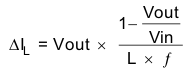
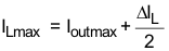
where
- f = Switching frequency
- L = Inductor value
- ΔIL= Peak-to-peak inductor ripple current
- ILmax = Maximum inductor current
Table 9-2 shows a list of possible inductors.
| INDUCTANCE [µH] | INDUCTOR SERIES | SIZE IMPERIAL (METRIC) | DIMENSIONS L × W × T | SUPPLIER(1) | |
|---|---|---|---|---|---|
| 0.47 | DFE18SAN_G0 | 0603 (1608) | 1.6 mm × 0.8 mm × 1.0 mm maximum | Murata | |
| 0.47 | HTEB16080F | 0603 (1608) | 1.6 mm × 0.8 mm × 0.6 mm maximum | Cyntec | |
| 0.47 | HTET1005FE | 0402 (1005) | 1.0 mm × 0.5 mm × 0.65 mm maximum | Cyntec | |
| 0.47 | TFM160808ALC | 0603 (1608) | 1.6 mm × 0.8 mm × 0.8 mm maximum | TDK | |