SLUSDU8F September 2019 – October 2023 TPS62860 , TPS62861
PRODUCTION DATA
- 1
- 1 Features
- 2 Applications
- 3 Description
- 4 Revision History
- 5 Device Comparison Table
- 6 Pin Configuration and Functions
- 7 Specifications
-
8 Detailed Description
- 8.1 Overview
- 8.2 Functional Block Diagram
- 8.3
Feature Description
- 8.3.1 Power Save Mode
- 8.3.2 Forced PWM Operation
- 8.3.3 Smart Enable and Shutdown (EN)
- 8.3.4 Soft Start
- 8.3.5 Output Voltage Selection (VSEL) for TPS62860x
- 8.3.6 Output Voltage Selection (VSEL and I2C)
- 8.3.7 Forced PWM Mode During Output Voltage Change
- 8.3.8 Undervoltage Lockout (UVLO)
- 8.3.9 Power Good (PG)
- 8.3.10 Switch Current Limit and Short Circuit Protection
- 8.3.11 Thermal Shutdown
- 8.3.12 Output Voltage Discharge
- 8.4 Programming
- 8.5 Register Map
- 9 Application and Implementation
- 10Device and Documentation Support
- 11Mechanical, Packaging, and Orderable Information
Package Options
Mechanical Data (Package|Pins)
- YCH|8
Thermal pad, mechanical data (Package|Pins)
Orderable Information
8.3.9 Power Good (PG)
The built-in power-good (PG) signal indicates that the output voltage has reached its target and the device is ready. The PG signal can be used for start-up sequencing of multiple rails or to indicate any overload behavior on the output. The PG pin is an open-drain output that requires a pullup resistor to any voltage up to the recommended input voltage level. PG is low when the device is turned off due to EN or thermal shutdown. VIN must remain present for the PG pin to stay LOW. When applying VIN the first time, PG stays HIGH until the first enabling of the device.
If the power-good output is not used, TI recommends to tie to GND or leave open.
| LOGIC SIGNALS | PG STATUS | ||||
|---|---|---|---|---|---|
| VI | EN-PIN | THERMAL SHUTDOWN | VOUT | DVS TRANSITION ACTIVE | |
| VI > UVLO | HIGH | NO | VOUT on target | NO | High Impedance |
| YES | LOW | ||||
| VOUT < target | x | LOW | |||
| YES | x | x | LOW | ||
| LOW | x | x | x | LOW | |
| VI < UVLO | x | x | x | x | Undefined |
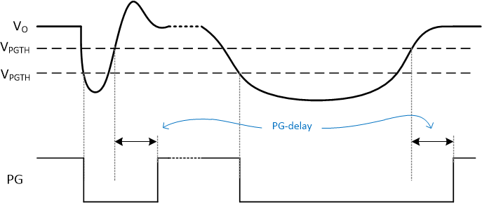
The PG indicator triggers immediately (after internal comparator delay) when VO crosses the lower VPGTH to indicate that the voltage has left the target setting. It features a delay after crossing the upper VPGTH when going high to make sure VO has reached the target again. Figure 8-2 sketches the behavior.
 Figure 8-2 Power Good Transient and De-glitch Behavior
The PG Indicator is by default pulled low during DVS transition of the output voltage without any blanking or delay time. Figure 8-2 shows an example of this behavior. After VO has reached the new target, the PG is again active as shown in Figure 8-2.