SLUSDU8F September 2019 – October 2023 TPS62860 , TPS62861
PRODUCTION DATA
- 1
- 1 Features
- 2 Applications
- 3 Description
- 4 Revision History
- 5 Device Comparison Table
- 6 Pin Configuration and Functions
- 7 Specifications
-
8 Detailed Description
- 8.1 Overview
- 8.2 Functional Block Diagram
- 8.3
Feature Description
- 8.3.1 Power Save Mode
- 8.3.2 Forced PWM Operation
- 8.3.3 Smart Enable and Shutdown (EN)
- 8.3.4 Soft Start
- 8.3.5 Output Voltage Selection (VSEL) for TPS62860x
- 8.3.6 Output Voltage Selection (VSEL and I2C)
- 8.3.7 Forced PWM Mode During Output Voltage Change
- 8.3.8 Undervoltage Lockout (UVLO)
- 8.3.9 Power Good (PG)
- 8.3.10 Switch Current Limit and Short Circuit Protection
- 8.3.11 Thermal Shutdown
- 8.3.12 Output Voltage Discharge
- 8.4 Programming
- 8.5 Register Map
- 9 Application and Implementation
- 10Device and Documentation Support
- 11Mechanical, Packaging, and Orderable Information
Package Options
Mechanical Data (Package|Pins)
- YCH|8
Thermal pad, mechanical data (Package|Pins)
Orderable Information
8.4.2 Standard- and Fast-Mode Protocol
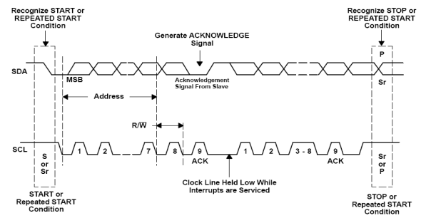
The master initiates data transfer by generating a start condition. The start condition is when a high-to-low transition occurs on the SDA line while SCL is high, as shown in Figure 8-3. All I2C-compatible devices recognize a start condition.
 Figure 8-3 START and STOP Conditions
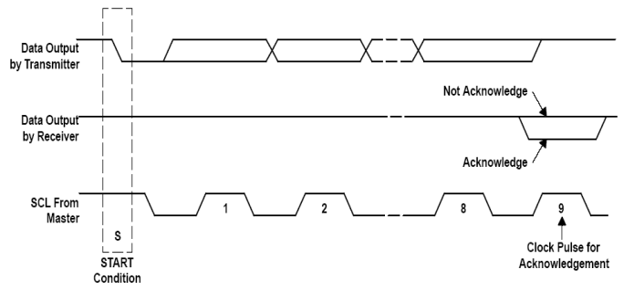
The master then generates the SCL pulses, and transmits the 7-bit address and the read/write direction bit R/W on the SDA line. During all transmissions, the master ensures that data is valid. A valid data condition requires the SDA line to be stable during the entire high period of the clock pulse (see Figure 8-4). All devices recognize the address sent by the master and compare it to their internal fixed addresses. Only the slave device with a matching address generates an acknowledge (see Figure 8-5) by pulling the SDA line low during the entire high period of the ninth SCL cycle. Upon detecting this acknowledge, the master knows that communication link with a slave has been established.
 Figure 8-4 Bit Transfer on the Serial Interface
The master generates further SCL cycles to either transmit data to the slave (R/W bit 1) or receive data from the slave (R/W bit 0). In either case, the receiver must acknowledge the data sent by the transmitter. An acknowledge signal can either be generated by the master or by the slave, depending on which one is the receiver. 9-bit valid data sequences consisting of 8-bit data and 1-bit acknowledge can continue as long as necessary.
To signal the end of the data transfer, the master generates a stop condition by pulling the SDA line from low to high while the SCL line is high (see Figure 8-3). This action releases the bus and stops the communication link with the addressed slave. All I2C-compatible devices must recognize the stop condition. Upon the receipt of a stop condition, all devices know that the bus is released, and the devices wait for a start condition followed by a matching address.
Attempting to read data from register addresses not listed in this section results in 00h being read out.
 Figure 8-5 Acknowledge on the I2C Bus
 Figure 8-6 Bus Protocol