SLVSD44A September   2017  – July 2018 TPS63710

PRODUCTION DATA.  

  1. Features
  2. Applications
  3. Description
    1.     Device Images
      1.      Typical Application
      2.      Efficiency vs output current for VOUT = -1.8V
  4. Revision History
  5. Pin Configuration and Functions
    1. Table 1. Pin Functions
  6. Specifications
    1. 6.1 Absolute Maximum Ratings
    2. 6.2 ESD Ratings
    3. 6.3 Recommended Operating Conditions
    4. 6.4 Thermal Information
    5. 6.5 Electrical Characteristics
    6. 6.6 Typical Characteristics
  7. Detailed Description
    1. 7.1 Overview
    2. 7.2 Functional Block Diagram
    3. 7.3 Feature Description
      1. 7.3.1 Low Noise Reference System
      2. 7.3.2 Duty Cycle
      3. 7.3.3 Enable
      4. 7.3.4 Undervoltage Lockout
      5. 7.3.5 Thermal Shutdown
      6. 7.3.6 Power Good Output
    4. 7.4 Device Functional Modes
      1. 7.4.1 Soft-Start
      2. 7.4.2 VOUT Discharge
      3. 7.4.3 Current Limit
      4. 7.4.4 CCP Capacitor Precharge
      5. 7.4.5 PWM Operation
  8. Application and Implementation
    1. 8.1 Application Information
    2. 8.2 Typical Application
      1. 8.2.1 Design Requirements
      2. 8.2.2 Detailed Design Procedure
        1. 8.2.2.1 Custom Design With WEBENCH® Tools
        2. 8.2.2.2 Setting the Output Voltage
        3. 8.2.2.3 Inductor Selection
        4. 8.2.2.4 Capacitor Selection
          1. 8.2.2.4.1 CCP Capacitor
          2. 8.2.2.4.2 Input Capacitor
          3. 8.2.2.4.3 Output Capacitor
      3. 8.2.3 Application Curves
        1. 8.2.3.1 Parameter Measurement Information
    3. 8.3 System Examples
      1. 8.3.1 Typical Application for Powering the Negative Rail of a Gallium Nitride (GaN) Power Amplifier
      2. 8.3.2 Typical Application for Powering the Negative Rail of an ADC or DAC
      3. 8.3.3 Typical Application for Laser Diode Bias
  9. Power Supply Recommendations
  10. 10Layout
    1. 10.1 Layout Guidelines
    2. 10.2 Layout Example
  11. 11Device and Documentation Support
    1. 11.1 Device Support
      1. 11.1.1 Custom Design With WEBENCH® Tools
      2. 11.1.2 Third-Party Products Disclaimer
    2. 11.2 Community Resources
    3. 11.3 Trademarks
    4. 11.4 Electrostatic Discharge Caution
    5. 11.5 Glossary
  12. 12Mechanical, Packaging, and Orderable Information

Package Options

Mechanical Data (Package|Pins)
Thermal pad, mechanical data (Package|Pins)
Orderable Information

Low Noise Reference System

The reference system in the TPS63710 uses an external filter capacitor on the CAP pin. This reduces the low-frequency (1/f) noise in a range from a lower limit up to around 100kHz. The lower limit is defined by the corner frequency of the RC filter from the internal 100-kΩ resistor and an external capacitor on the CAP pin. The corner frequency is defined by Equation 1.

Equation 1. TPS63710 equation_fc.gif

In order to minimize the noise on the output voltage, the TPS63710 uses an architecture where the output voltage setting is done by changing the reference voltage which then is filtered. The gain stage therefore does not have to have a large gain in order to not increase the noise level. VBG is the internal bandgap reference voltage, optimized for low noise. Its output voltage is amplified and inverted and then filtered. The voltage on the CAP pin is the reference for the gain stage. The connection from CAP to the external capacitor should be as short as possible and be kept away from noisy traces. The gain stage has a small gain of 1/0.9. The voltage at VREF is negative and lower than the output voltage by the gain factor of the gain stage. Please also see Setting the Output Voltage. Figure 8 shows the low noise architecture.
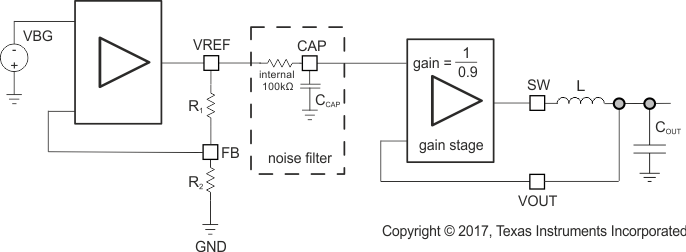
TPS63710 TPS63710_principle.gifFigure 8. Low Noise Architecture