SLVS927F March 2009 – July 2018 TPS65023-Q1
PRODUCTION DATA.
- 1 Features
- 2 Applications
- 3 Description
- 4 Revision History
- 5 Description (continued)
- 6 Pin Configuration and Functions
- 7 Specifications
-
8 Detailed Description
- 8.1 Overview
- 8.2 Functional Block Diagram
- 8.3 Feature Description
- 8.4 Device Functional Modes
- 8.5 Programming
- 8.6
Register Maps
- 8.6.1 VERSION Register (address: 00h) Read-Only
- 8.6.2 PGOODZ Register (address: 01h) Read-Only
- 8.6.3 MASK Register (address: 02h)
- 8.6.4 REG_CTRL Register (address: 03h)
- 8.6.5 CON_CTRL Register (address: 04h)
- 8.6.6 CON_CTRL2 Register (address: 05h)
- 8.6.7 DEFCORE Register (address: 06h)
- 8.6.8 DEFSLEW Register (address: 07h)
- 8.6.9 LDO_CTRL Register (address: 08h)
- 9 Application and Implementation
- 10Power Supply Recommendations
- 11Layout
- 12Device and Documentation Support
- 13Mechanical, Packaging, and Orderable Information
Package Options
Mechanical Data (Package|Pins)
Thermal pad, mechanical data (Package|Pins)
Orderable Information
8.4.2 Power-Save Mode Operation (PSM)
As the load current decreases, the converters enter the power-save mode of operation. During PSM, the converters operate in a burst mode (PFM mode) with a frequency between 750 kHz and 2.25 MHz, nominal, for one burst cycle. However, the frequency between different burst cycles depends on the actual load current and is typically far less than the switching frequency, with a minimum quiescent current to maintain high efficiency.
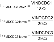
To optimize the converter efficiency at light load, the average current is monitored, and if in PWM mode the inductor current remains below a certain threshold, then PSM is entered. The typical threshold to enter PSM is calculated as follows:

During PSM, the output voltage is monitored with a comparator, and by maximum skip burst duration. As the output voltage falls below the threshold, set to the nominal VO, the P-channel switch turns on, and the converter effectively delivers a constant current defined as follows.

If the load is below the delivered current, then the output voltage rises until the same threshold is crossed in the other direction. All switching activity ceases, reducing the quiescent current to a minimum until the output voltage has again dropped below the threshold. The power-save mode is exited, and the converter returns to PWM mode if either of the following conditions is met:
- the output voltage drops 2% below the nominal VO due to increasing load current
- the PFM burst time exceeds 16 × 1 / fS (7.11 μs typical).
These control methods reduce the quiescent current to typically 14 μA per converter, and the switching activity to a minimum, thus achieving the highest converter efficiency. Setting the comparator thresholds at the nominal output voltage at light load current results in a low output-voltage ripple. The ripple depends on the comparator delay and the size of the output capacitor. Increasing capacitor values makes the output ripple tend to zero. The PSM is disabled through the I2C interface to force the individual converters to stay in fixed-frequency PWM mode.