SLVS843B December   2008  – May 2018 TPS650250

PRODUCTION DATA.  

  1. Features
  2. Applications
  3. Description
    1.     Detailed Block Diagram
  4. Revision History
  5. Pin Configuration and Functions
    1.     Pin Functions
  6. Specifications
    1. 6.1  Absolute Maximum Ratings
    2. 6.2  ESD Ratings
    3. 6.3  Recommended Operating Conditions
    4. 6.4  Thermal Information
    5. 6.5  Dissipation Ratings
    6. 6.6  Electrical Characteristics
    7. 6.7  Electrical Characteristics VDCDC1
    8. 6.8  Electrical Characteristics VDCDC2
    9. 6.9  Electrical Characteristics VDCDC3
    10. 6.10 Typical Characteristics
  7. Detailed Description
    1. 7.1 Overview
    2. 7.2 Functional Block Diagram
    3. 7.3 Feature Description
      1. 7.3.1 Step-Down Converters, VDCDC1, VDCDC2 AND VDCDC3
      2. 7.3.2 Power Save Mode Operation
      3. 7.3.3 Soft Start
      4. 7.3.4 100% Duty Cycle Low Dropout Operation
      5. 7.3.5 Low Dropout Voltage Regulators
      6. 7.3.6 Undervoltage Lockout
      7. 7.3.7 PWRFAIL
    4. 7.4 Device Functional Modes
  8. Application and Implementation
    1. 8.1 Application Information
    2. 8.2 Typical Application
      1. 8.2.1 Typical Configuration For The Samsung Processor S3C6400-533MHz
      2. 8.2.2 Design Requirements
      3. 8.2.3 Detailed Design Procedure
        1. 8.2.3.1 Inductor Selection for the DCDC Converters
        2. 8.2.3.2 Output Capacitor Selection
        3. 8.2.3.3 Input Capacitor Selection
        4. 8.2.3.4 Output Voltage Selection
        5. 8.2.3.5 Voltage Change on VDCDC3
        6. 8.2.3.6 Vdd_alive Output
        7. 8.2.3.7 LDO1 and LDO2
        8. 8.2.3.8 Vcc-Filter
      4. 8.2.4 Application Curves
  9. Power Supply Recommendations
  10. 10Layout
    1. 10.1 Layout Guidelines
    2. 10.2 Layout Example
  11. 11Device and Documentation Support
    1. 11.1 Device Support
      1. 11.1.1 Third-Party Products Disclaimer
      2. 11.1.2 Development Support
    2. 11.2 Documentation Support
      1. 11.2.1 Related Documentation
    3. 11.3 Receiving Notification of Documentation Updates
    4. 11.4 Community Resources
    5. 11.5 Trademarks
    6. 11.6 Electrostatic Discharge Caution
    7. 11.7 Glossary
  12. 12Mechanical, Packaging, and Orderable Information

Package Options

Mechanical Data (Package|Pins)
Thermal pad, mechanical data (Package|Pins)
Orderable Information

Application Curves

The application curves were taken using the following inductor/output capacitor combinations

CONVERTER INDUCTOR OUTPUT CAPACITOR OUTPUT CAPACITOR VALUE
DCDC1 VLCF4020-3R3 C2012X5R0J226M 22 μF
DCDC2 VLCF4020-2R2 C2012X5R0J226M 22 μF
DCDC3 LPS3010-222 C2012X5R0J226M 22 μF

Table 7. Table of Application Curves

FIGURE
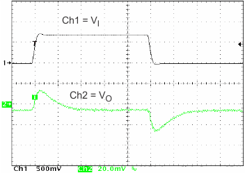
Line transient response VDCDC1 Figure 9
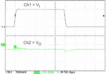
Line transient response VDCDC2 Figure 10
Line transient response VDCDC3 Figure 11
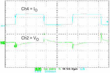
Load transient response VDCDC1 Figure 12
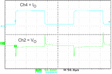
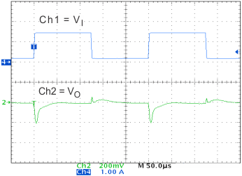
Load transient response VDCDC2 Figure 13
Load transient response VDCDC3 Figure 14
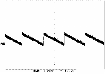
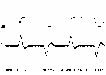
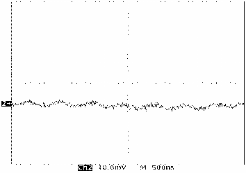
Output voltage ripple DCDC2; PFM mode Figure 15
Output voltage ripple DCDC2; PWM mode Figure 16
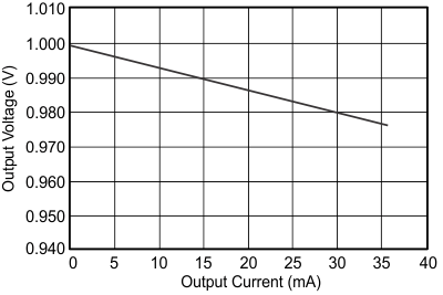
Load regulation for Vdd_alive Figure 17
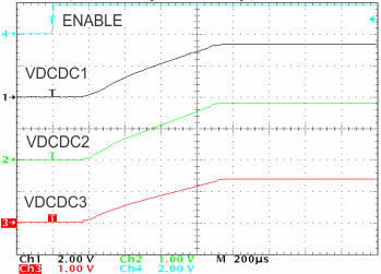
Start-up VDCDC1 to VDCDC3 Figure 18
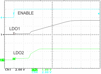
Start-up LDO1 and LDO2 Figure 19
TPS650250 lin_trn_res_lvs774.gif
Figure 9. VDCDC1 Line Transient Response
TPS650250 lin2_trn_res_lvs774.gif
Figure 11. VDCDC3 Line Transient Response
TPS650250 ld_trn_res_lvs774.gif
Figure 13. VDCDC2 Load Transient Response
TPS650250 vdcdc2_vo1_lvs774.gif
Figure 15. VDCDC2 Output Voltage Ripple
TPS650250 vo_io_lvs843.gif
Figure 17. VDD_ALIVE Output Voltage vs Output Current
TPS650250 ldo_startup_lvs774.gif
Figure 19. Startup LDO1 and LDO2
TPS650250 vdcdc2_lt_lvs774.gif
Figure 10. VDCDC2 Line Transient Response
TPS650250 ld3_trn_lvs774.gif
Figure 12. VDCDC1 Load Transient Response
TPS650250 ld2_trn_res_lvs774.gif
Figure 14. VDCDC3 Load Transient Response
TPS650250 vdcdc2_vo3_lvs774.gif
Figure 16. VDCDC2 Output Voltage Ripple
TPS650250 startup2_lvs774.gif
Figure 18. Startup VDCDC1, VDCDC2, VDCDC3