SWCS138E June 2017 – December 2022 TPS650864
PRODUCTION DATA
- 1 Features
- 2 Applications
- 3 Description
- 4 Revision History
- 5 Device Comparison Table
- 6 Pin Configuration and Functions
-
7 Specifications
- 7.1 Absolute Maximum Ratings
- 7.2 ESD Ratings
- 7.3 Recommended Operating Conditions
- 7.4 Thermal Information
- 7.5 Electrical Characteristics: Total Current Consumption
- 7.6 Electrical Characteristics: Reference and Monitoring System
- 7.7 Electrical Characteristics: Buck Controllers
- 7.8 Electrical Characteristics: Synchronous Buck Converters
- 7.9 Electrical Characteristics: LDOs
- 7.10 Electrical Characteristics: Load Switches
- 7.11 Digital Signals: I2C Interface
- 7.12 Digital Input Signals (CTLx)
- 7.13 Digital Output Signals (IRQB, GPOx)
- 7.14 Timing Requirements
- 7.15 Switching Characteristics
- 7.16 Typical Characteristics
-
8 Detailed Description
- 8.1 Overview
- 8.2 Functional Block Diagram
- 8.3 TPS6508640 Design and Settings
- 8.4 TPS65086401 Design and Settings
- 8.5 TPS6508641 Design and Settings
- 8.6 TPS65086470 Design and Settings
- 8.7 SMPS Voltage Regulators
- 8.8 LDOs and Load Switches
- 8.9 Power Goods (PGOOD or PG) and GPOs
- 8.10 Power Sequencing and VR Control
- 8.11 Device Functional Modes
- 8.12 I2C Interface
- 8.13
Register Maps
- 8.13.1 Register Map Summary
- 8.13.2 DEVICEID1: 1st PMIC Device and Revision ID Register (offset = 00h) [reset = X]
- 8.13.3 DEVICEID2: 2nd PMIC Device and Revision ID Register (offset = 01h) [reset = X]
- 8.13.4 IRQ: PMIC Interrupt Register (offset = 02h) [reset = 0000 0000]
- 8.13.5 IRQ_MASK: PMIC Interrupt Mask Register (offset = 03h) [reset = 1111 1111]
- 8.13.6 PMICSTAT: PMIC Status Register (offset = 04h) [reset = 0000 0000]
- 8.13.7 SHUTDNSRC: PMIC Shut-Down Event Register (offset = 05h) [reset = 0000 0000]
- 8.13.8 BUCK1CTRL: BUCK1 Control Register (offset = 20h) [reset = X]
- 8.13.9 BUCK2CTRL: BUCK2 Control Register (offset = 21h) [reset = X]
- 8.13.10 BUCK3DECAY: BUCK3 Decay Control Register (offset = 22h) [reset = X]
- 8.13.11 BUCK3VID: BUCK3 VID Register (offset = 23h) [reset = X]
- 8.13.12 BUCK3SLPCTRL: BUCK3 Sleep Control VID Register (offset = 24h) [reset = X]
- 8.13.13 BUCK4CTRL: BUCK4 Control Register (offset = 25h) [reset = X]
- 8.13.14 BUCK5CTRL: BUCK5 Control Register (offset = 26h) [reset = X]
- 8.13.15 BUCK6CTRL: BUCK6 Control Register (offset = 27h) [reset = X]
- 8.13.16 LDOA2CTRL: LDOA2 Control Register (offset = 28h) [reset = X]
- 8.13.17 LDOA3CTRL: LDOA3 Control Register (offset = 29h) [reset = X]
- 8.13.18 DISCHCTRL1: 1st Discharge Control Register (offset = 40h) [reset = X]
- 8.13.19 DISCHCTRL2: 2nd Discharge Control Register (offset = 41h) [reset = X]
- 8.13.20 DISCHCTRL3: 3rd Discharge Control Register (offset = 42h) [reset = X]
- 8.13.21 PG_DELAY1: 1st Power Good Delay Register (offset = 43h) [reset = X]
- 8.13.22 FORCESHUTDN: Force Emergency Shutdown Control Register (offset = 91h) [reset = 0000 0000]
- 8.13.23 BUCK1SLPCTRL: BUCK1 Sleep Control Register (offset = 92h) [reset = X]
- 8.13.24 BUCK2SLPCTRL: BUCK2 Sleep Control Register (offset = 93h) [reset = X]
- 8.13.25 BUCK4VID: BUCK4 VID Register (offset = 94h) [reset = X]
- 8.13.26 BUCK4SLPVID: BUCK4 Sleep VID Register (offset = 95h) [reset = X]
- 8.13.27 BUCK5VID: BUCK5 VID Register (offset = 96h) [reset = X]
- 8.13.28 BUCK5SLPVID: BUCK5 Sleep VID Register (offset = 97h) [reset = X]
- 8.13.29 BUCK6VID: BUCK6 VID Register (offset = 98h) [reset = X]
- 8.13.30 BUCK6SLPVID: BUCK6 Sleep VID Register (offset = 99h) [reset = X]
- 8.13.31 LDOA2VID: LDOA2 VID Register (offset = 9Ah) [reset = X]
- 8.13.32 LDOA3VID: LDOA3 VID Register (offset = 9Bh) [reset = X]
- 8.13.33 BUCK123CTRL: BUCK1-3 Control Register (offset = 9Ch) [reset = X]
- 8.13.34 PG_DELAY2: 2nd Power Good Delay Register (offset = 9Dh) [reset = X]
- 8.13.35 SWVTT_DIS: SWVTT Disable Register (offset = 9Fh) [reset = X]
- 8.13.36 I2C_RAIL_EN1: 1st VR Pin Enable Override Register (offset = A0h) [reset = X]
- 8.13.37 I2C_RAIL_EN2/GPOCTRL: 2nd VR Pin Enable Override and GPO Control Register (offset = A1h) [reset = X]
- 8.13.38 PWR_FAULT_MASK1: 1st VR Power Fault Mask Register (offset = A2h) [reset = X]
- 8.13.39 PWR_FAULT_MASK2: 2nd VR Power Fault Mask Register (offset = A3h) [reset = X]
- 8.13.40 GPO1PG_CTRL1: 1st GPO1 PG Control Register (offset = A4h) [reset = X]
- 8.13.41 GPO1PG_CTRL2: 2nd GPO1 PG Control Register (offset = A5h) [reset = X]
- 8.13.42 GPO4PG_CTRL1: 1st GPO4 PG Control Register (offset = A6h) [reset = X]
- 8.13.43 GPO4PG_CTRL2: 2nd GPO4 PG Control Register (offset = A7h) [reset = X]
- 8.13.44 GPO2PG_CTRL1: 1st GPO2 PG Control Register (offset = A8h) [reset = X]
- 8.13.45 GPO2PG_CTRL2: 2nd GPO2 PG Control Register (offset = A9h) [reset = X]
- 8.13.46 GPO3PG_CTRL1: 1st GPO3 PG Control Register (offset = AAh) [reset = X]
- 8.13.47 GPO3PG_CTRL2: 2nd GPO3 PG Control Register (offset = ABh) [reset = X]
- 8.13.48 MISCSYSPG Register (offset = ACh) [reset = X]
- 8.13.49 LDOA1_SWB2_CTRL: LDOA1 and SWB2 Control Register (offset = AEh) [reset = X]
- 8.13.50 PG_STATUS1: 1st Power Good Status Register (offset = B0h) [reset = 0000 0000]
- 8.13.51 PG_STATUS2: 2nd Power Good Status Register (offset = B1h) [reset = 0000 0000]
- 8.13.52 PWR_FAULT_STATUS1: 1st Power Fault Status Register (offset = B2h) [reset = 0000 0000]
- 8.13.53 PWR_FAULT_STATUS2: 2nd Power Fault Status Register (offset = B3h) [reset = 0000 0000]
- 8.13.54 TEMPCRIT: Temperature Fault Status Register (offset = B4h) [reset = 0000 0000]
- 8.13.55 TEMPHOT: Temperature Hot Status Register (offset = B5h) [reset = 0000 0000]
- 8.13.56 OC_STATUS: Overcurrent Fault Status Register (offset = B6h) [reset = 0000 0000]
-
9 Applications, Implementation, and Layout
- 9.1 Application Information
- 9.2 Typical Application
- 9.3 Power Supply Coupling and Bulk Capacitors
- 9.4 Do's and Don'ts
- 10Device and Documentation Support
- 11Mechanical, Packaging, and Orderable Information
Package Options
Mechanical Data (Package|Pins)
- RSK|64
Thermal pad, mechanical data (Package|Pins)
- RSK|64
Orderable Information
9.2.2.1.2 Selecting the Output Capacitors
TI recommends using ceramic capacitors with low ESR values to provide the lowest output voltage ripple. The output capacitor requires an X7R or an X5R dielectric. Y5V and Z5U dielectric capacitors, aside from their wide variation in capacitance over temperature, become resistive at high frequencies.
At light load currents, the controller operates in PFM mode, and the output voltage ripple is dependent on the output-capacitor value and the PFM peak inductor current. Higher output-capacitor values minimize the voltage ripple in PFM mode. To achieve specified regulation performance and low output voltage ripple, the DC-bias characteristic of ceramic capacitors must be considered. The effective capacitance of ceramic capacitors drops with increasing DC bias voltage.
TI recommends the use of small ceramic capacitors placed between the inductor and load with many vias to the PGND plane for the output capacitors of the BUCK controllers. This solution typically provides the smallest and lowest cost solution available for D-CAP2 controllers.
The selection of the output capacitor is typically driven by the output transient response. Equation 7 and Equation 8 provide a rough estimate of the minimum required capacitance to ensure proper transient response. Because the transient response is significantly affected by the board layout, some experimentation is expected in order to confirm that values derived in this section are applicable to any particular use case. These are not meant to be an absolute requirement, but rather a rough starting point. Alternatively, some known combination values from which to begin are provided in Table 9-1. VUNDER and VOVER values should be greater than or equal to 3% of VOUT setting in order for equations to be meaningful. The equations provide some margin so that actual capacitance requirement may be lower than calculated.
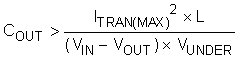
where
- ITRAN(max) is the maximum load current step
- L is the chosen inductance
- VIN is the maximum input voltage
- VOUT is the minimum programmed output voltage
- VUNDER is the maximum allowable undershoot from programmed voltage
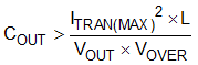
where
- VOVER is the maximum allowable overshoot from programmed voltage
Another key performance factor can be the ripple voltage while in pulsed frequency modulation mode, also known as discontinuous conduction mode. At light load, the controller will disable the low side FET once it detects a zero-crossing event on the inductor current. It will stay disabled until VOUT crosses below the set VID threshold. This architecture allows significant power savings at light load conditions by minimizing power loss through the low side FET and through switching. The disadvantage is that there is higher voltage ripple since the ripple current is only positive. Additionally, for even higher efficiency, TON(PFM) for this device is typically 80% longer than TON(PWM), which can be calculated by dividing the duty cycle by the switching frequency. An estimate for the required capacitance for a given allowable ripple voltage at light load is shown in Equation 9. ESR of the output capacitor is neglected here because ceramic capacitors, which typically have low ESR, are recommended. VOVER should not be set lower than 3% of VOUT value.
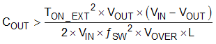
where
- TON_EXT is the PFM on time extension constant, 1.8 unless otherwise noted in the part number specific section
- VOUT is the maximum programmed output voltage
- VIN is the maximum input voltage
- fSW is the typical switching frequency when loaded, 1 MHz unless otherwise noted
- VOVER is the maximum allowable overshoot from programmed voltage
- L is the chosen inductance
In cases where the transient current change is very low and ripple voltage allowance is large, the DC stability may become important. DCAP2 is a very stable architecture so this value is likely to be the smallest of those calculated. Equation 10 approximates the amount of capacitance necessary to maintain DC stability. Again, this is provided as a starting point; actual values will vary on a board-to-board case.
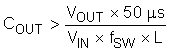
where
- VOUT is the maximum programmed output voltage
- 50 µs is based on internal ramp setup
- VIN is the minimum input voltage
- fSW is the typical switching frequency
- L is the chosen inductance
Choosing the maximum valuable between Equation 7, Equation 8, Equation 9, and Equation 10 is recommended as a starting point to get the desired performance. All equations are estimates and have not been validated at all variable corners. Removing excess capacitance or adding extra capacitance may be necessary during board evaluation. Testing can typically be performed on the evaluation module or on prototype boards.
| ITRAN(max) (A) | L (µH) | VOUT (V) | VUNDER (V) | VOVER (V) | COUT(µF) |
|---|---|---|---|---|---|
| 3.5 | 0.47 | 1 | 0.05 | 0.05 | 110 |
| 4 | 0.47 | 1 | 0.05 | 0.05 | 220 |
| 5 | 0.47 | 1.35 | 0.068 | 0.068 | 220 |
| 8 | 0.33 | 1 | 0.05 | 0.06 | 440 |
| 20 | 0.22 | 1 | 0.05 | 0.16 | 550 |