SLVSBX4C June 2013 – May 2017 TPS65150-Q1
PRODUCTION DATA.
- 1 Features
- 2 Applications
- 3 Description
- 4 Revision History
- 5 Pin Configuration and Functions
- 6 Specifications
- 7 Detailed Description
-
8 Application and Implementation
- 8.1 Application Information
- 8.2
Typical Application
- 8.2.1 Design Requirements
- 8.2.2
Detailed Design Procedure
- 8.2.2.1 Boost Converter Design Procedure
- 8.2.2.2 Rectifier Diode Selection
- 8.2.2.3 Setting the Output Voltage
- 8.2.2.4 Output Capacitor Selection
- 8.2.2.5 Input Capacitor Selection
- 8.2.2.6 Compensation
- 8.2.2.7 Negative Charge Pump
- 8.2.2.8 Positive Charge Pump
- 8.2.2.9 Gate Voltage Shaping
- 8.2.2.10 Power-On Sequencing
- 8.2.2.11 Fault Delay
- 8.2.3 Application Curves
- 8.3 System Examples
- 9 Power Supply Recommendations
- 10Layout
- 11Device and Documentation Support
- 12Mechanical, Packaging, and Orderable Information
Package Options
Mechanical Data (Package|Pins)
- PWP|24
Thermal pad, mechanical data (Package|Pins)
- PWP|24
Orderable Information
7 Detailed Description
7.1 Overview
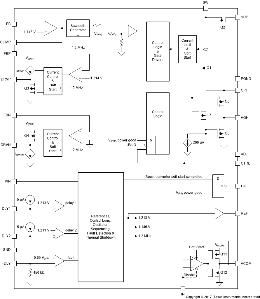
The TPS65150-Q1 device is a complete bias supply for LCD displays. The device generates supply voltages for the source driver and gate driver ICs in the display as well as generating the common plane voltage of the display (VCOM). The device also features a gate-voltage shaping function that can be used to reduce image sticking and improve picture quality. The use of external components to control power-up sequencing, fault detection time, and boost converter compensation allows the device to be optimized for a variety of displays.
The device has been designed to work from input supply voltages as low as 1.8 V and is therefore ideal for use in applications where it is supplied from fixed 2.5-V, 3.3-V, or 5-V supplies.
7.3 Feature Description
7.3.1 Boost Converter
Figure 8 shows a simplified block diagram of the boost converter.
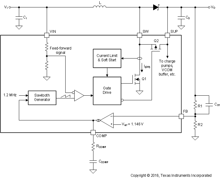 Figure 8. Boost Converter Block Diagram
The boost converter uses a unique fast-response voltage-mode controller scheme with input feedforward to achieve excellent line and load regulation, while still allowing the use of small external components. The use of external compensation adds flexibility and allows the response of the boost converter to be optimized for a wide range of external components.
The TPS65150-Q1 device uses a virtual-synchronous topology that allows the boost converter to operate in continuous conduction mode (CCM) even at light loads. This is achieved by including a small MOSFET (Q2) in parallel with the external rectifier diode. Under light-load conditions, Q2 allows the inductor current to become negative, maintaining operation in CCM. By operating always in CCM, boost converter compensation is simplified, ringing on the SW pin at low loads is avoided, and additional charge pump stages can be driven by the SW pin. The boost converter duty cycle is given by Equation 1.

where
- η is the boost converter efficiency (either taken from data in Application Curves or a worst-case assumption of 75%),
- VI is the boost converter input supply voltage, and
- VO is the boost converter output voltage.
Use Equation 2 to calculate the boost converter peak switch current.

where
- f = 1.2 MHz (the boost converter switching frequency),
- IO is the boost converter output current, and
- L is the boost converter inductance.
7.3.1.1 Setting the Boost Converter Output Voltage
The boost converter output voltage is set by the R1/R2 resistor divider, and is calculated using Equation 3.

where
- Vref = 1.146 V (the boost converter internal reference voltage).
To minimize quiescent current consumption, the value of R1 should be in the range of 100 kΩ to 1 MΩ.
7.3.1.2 Boost Converter Rectifier Diode
The reverse voltage rating of the diode must be higher than the maximum output voltage of the converter, and its average forward current rating must be higher than the output current of the boost converter. Use Equation 4 to calculate the rectifier diode repetitive peak forward current.

Use Equation 5 to calculate the power dissipated in the rectifier diode.

where
- VF is the rectifier diode forward voltage.
The main diode parameters affecting converter efficiency are its forward voltage and reverse leakage current, and both should be as low as possible.
7.3.1.3 Choosing the Boost Converter Output Capacitance
The output capacitance of the boost converter smooths the output voltage and supplies transient output current demands that are outside the loop bandwidth of the converter. Generally speaking, larger output currents or smaller input supply voltages require larger output capacitances. Use Equation 6 to calculate the output voltage ripple of the boost converter.

where
- CO is the boost converter output capacitance.
7.3.1.4 Compensation
The boost converter requires a series R-C network connected between the COMP pin and ground to compensate its feedback loop. The COMP pin is the output of the boost converter's error amplifier, and the compensation capacitor determines the amplifier's low-frequency gain and the resistor its high-frequency gain. Because the converter gain changes with the input voltage, different compensation capacitors may be required: lower input voltages require a higher gain, and therefore a smaller compensation capacitor value. If an input supply voltage of the application changes (for example, if the TPS65150-Q1 device is supplied from a battery), choose compensation components suitable for a supply voltage midway between the minimum and maximum values. In all cases, verify that the values selected are suitable by performing transient tests over the full range of operating conditions.
Table 2. Recommended Compensation Components for Different Input Supply Voltages
| VI | CCOMP | RCOMP | FEED-FORWARD ZERO CUT-OFF FREQUENCY |
|---|---|---|---|
| 2.5 V | 470 pF | 68 kΩ | 8.8 kHz |
| 3.3 V | 470 pF | 33 kΩ | 7.8 kHz |
| 5 V | 2.2 nF | 0 kΩ | 11.2 kHz |
A feed-forward capacitor CFF in parallel with the upper feedback resistor R1 adds an additional zero to the loop response, which improves transient performance. Table 2 suggests suitable values for the cut-off frequency of the feedforward zero; however, these are only guidelines. In any application, variations in input supply voltage, inductance, and output capacitance all affect circuit operation, and the optimum value must be verified with transient tests before being finalized.
The cut-off frequency of the feed-forward zero is determined using Equation 7.

where
- fco is the cutoff frequency of the feedforward zero formed by R1 and CFF.
7.3.1.5 Soft Start
The boost converter features a soft-start function that limits the current drawn from the input supply during start-up. During the first 2048 switching cycles, the switch current of the boost converter is limited to 40% of its maximum value; during the next 2048 cycles, it is limited to 60% of its maximum value; and after that it is as high as it must be to regulate the output voltage (up to 100% of the maximum). In typical applications, this results in a start-up time of about 5 ms (see Figure 9).
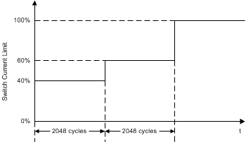 Figure 9. Boost Converter Switch Current Limit During Soft-Start
7.3.1.6 Gate Drive Signal
The GD pin provides a signal to control an external P-channel enhancement MOSFET, allowing the output of the boost converter to be isolated from its input when disabled (see Figure 36). The GD pin is an open-drain type whose output is latched low as soon as the output voltage of the boost converter reaches its power-good threshold. The GD pin goes high impedance whenever the input voltage falls below the undervoltage lockout threshold or the device shuts down as the result of a fault condition (see Adjustable Fault Delay).
7.3.2 Negative Charge Pump
Figure 10 shows a simplified block diagram of the negative charge pump.
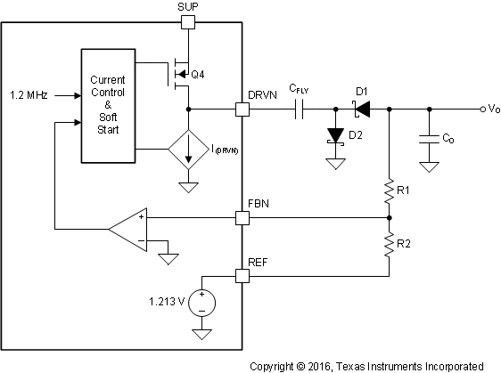 Figure 10. Negative Charge Pump Block Diagram
The negative charge pump operates with a fixed frequency of 1.2 MHz and a 50% duty cycle in two distinct phases. During the charge phase, transistor Q4 is turned on, controlled current source I(DRVN) is turned off, and flying capacitance CFLY charges up to approximately V(SUP). During the discharge phase, Q4 is turned off, I(DRVN) is turned on, and a negative current of I(DRVN) flows through D1 to the output. The output voltage is fed back through R1 and R2 to an error amplifier that controls I(DRVN) so that the output voltage is regulated at the correct value.
7.3.2.1 Negative Charge Pump Output Voltage
The negative charge pump output voltage is set by resistors R1 and R2 and is given by Equation 8.

where
- V(REF) = 1.213 V (the voltage on the REF pin).
Resistor R2 should be in the range 39 kΩ to 150 kΩ. Smaller values load the REF pin too heavily and larger values may cause stability problems.
7.3.2.2 Negative Charge Pump Flying Capacitance
The flying capacitance transfers charge from the SUP pin to the negative charge pump output. TI recommends a flying capacitor of at least 100 nF for output currents up to 20 mA. Smaller values can be used with smaller output currents.
7.3.2.3 Negative Charge Pump Output Capacitance
The output capacitor smooths the discontinuous current delivered by the flying capacitor to generate a DC output voltage. In general, higher output currents require larger output capacitances. Use Equation 9 to calculate the negative charge pump output voltage ripple.

where
- IO is the negative charge pump output current,
- CO is the negative charge pump output capacitance, and
- f = 1.2 MHz (the negative charge pump switching frequency).
7.3.2.4 Negative Charge Pump Diodes
The average forward current of both diodes is equal to the negative charge pump output current. If the recommended flying capacitor (or larger) is used, the repetitive peak forward current in D1 and D2 is equal to twice the output current.
7.3.3 Positive Charge Pump
Figure 11 shows a simplified block diagram of the positive charge pump, which works in a similar way to the negative charge pump except that the positions of the current source IDRVP and the MOSFET Q3 are reversed.
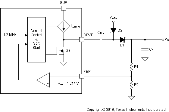 Figure 11. Positive Charge Pump Block Diagram
If higher output voltages are required another charge pump stage can be added to the output, as shown in Figure 34 at the end of the data sheet.
7.3.3.1 Positive Charge Pump Output Voltage
The positive charge pump output voltage is set by resistors R1 and R2 and is calculated using Equation 10.

where
- Vref = 1.214 V (the positive charge pump reference voltage).
TI recommends choosing a value for R2 not greater than 1 MΩ.
7.3.3.2 Positive Charge Pump Flying Capacitance
The flying capacitance transfers charge from the SUP pin to the charge pump output. TI recommends a flying capacitor of at least 330 nF The minimum recommended flying capacitance for the positive charge pump is larger than for the negative charge pump because the r for output currents up to 20 mA. Smaller values can be used with smaller output currents.
7.3.3.3 Positive Charge Pump Output Capacitance
The output voltage ripple of the positive charge pump is given by Equation 11.

where
- IO is the output current of the positive charge pump,
- CO is the output capacitance of the positive charge pump, and
- f = 1.2 MHz (the switching frequency of the positive charge pump).
7.3.3.4 Positive Charge Pump Diodes
The average forward current of both diodes is equal to the positive charge pump output current. If the recommended flying capacitance (or larger) is used, the repetitive peak forward current in D1 and D2 equal to twice the output current.
7.3.4 Power-On Sequencing, DLY1, DLY2
The boost converter starts as soon as the input supply voltage exceeds the rising UVLO threshold. The negative charge pump starts td(DLY1) seconds after the boost converter output voltage has reached its final value, and the positive charge pump starts td(DLY2) seconds after the output of the negative charge pump has reached its final value. The VCOM buffer starts up as soon as the output voltage of the positive charge pump (V(CPI)) has reached its final value.
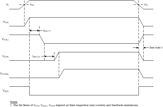 Figure 12. Start-Up Sequencing With CTRL = High
The delay times td(DLY1) and td(DLY2) are set by the capacitors connected to the DLY1 and DLY2 pins respectively. Each of these pins is connected to its own 5-µA current source (I(DLY1) and I(DLY2)) that causes the voltage on the external capacitor to ramp up linearly. The delay time is defined by how long it takes the voltage on the external capacitor to reach the reference voltage, and is given by Equation 12.

where
- Vref = 1.213 V (the internal reference voltage),
- I(DLY1) = 5 µA (the DLY1 pin output current), and
- I(DLY2) = 5 µA (the DLY2 pin output current).
7.3.5 Gate Voltage Shaping
The gate voltage shaping function can be used to reduce crosstalk between LCD pixels by reducing the gate drivers’ input supply voltage between lines. Figure 13 shows a simplified block diagram of the gate voltage shaping function. Gate voltage shaping is controlled by a logic-level signal applied to the CTRL pin. When CTRL is high, Q5 and Q7 are on and Q6 is off, and the output of the positive charge pump is connected to the VGH pin. When CTRL is low, Q5 and Q7 are off and Q6 is on. Q6 operates as a source follower and tracks the voltage on the ADJ pin, which ramps down linearly as the current sink I(ADJ) discharges the external capacitor CADJ (see Figure 14). The peak-to-peak voltage on the VGH pin is determined by the value of CADJ and the duration of the low level applied to the CTRL pin, and is calculated using Equation 13.

where
- I(ADJ) = 200 µA (ADJ pin output current),
- tw(CTRL) is the duration of the low-level signal connected to the CTRL pin, and
- CADJ is the capacitance connected to the ADJ pin.
When the input supply voltage is below the UVLO threshold or the device enters a shutdown condition because of a fault on one or more of its outputs, Q5 and Q6 turn off and the VGH pin is high impedance.
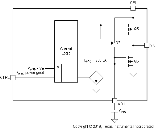 Figure 13. Gate Voltage Shaping Block Diagram
 Figure 14. Gate Voltage Shaping Timing
7.3.6 VCOM Buffer
The VCOM Buffer is a transconductance amplifier designed to drive capacitive loads. The IN pin is the input of the VCOM buffer. The VCOM buffer features a soft-start function that reduces the current drawn from the SUP pin when the amplifier starts up.
If the VCOM buffer is not required for certain applications, it is possible to shut down the VCOM buffer by connecting IN to ground, reducing the overall quiescent current. The IN pin cannot be pulled dynamically to ground during operation.
7.3.7 Protection
7.3.7.1 Boost Converter Overvoltage Protection
The boost converter features an overvoltage protection function that monitors the voltage on the SUP pin and forces the TPS65150-Q1 device to enter fault mode if the boost converter output voltage exceeds the overvoltage threshold.
7.3.7.2 Adjustable Fault Delay
The TPS65150-Q1 device detects a fault condition and shuts down if the boost converter output or either of the charge pump outputs falls out of regulation for longer than the fault delay time td(FDLY). Fault conditions are detected by comparing the voltage on the feedback pins with the internal power-good thresholds. Outputs that fall below their power-good threshold but recover within less than td(FDLY) seconds are not detected as faults and the device does not shut down in such cases. The output fault detection function is active during start-up, so the device shuts down if any of its outputs fails to reach its power-good threshold during start-up. Shut-down following an output voltage fault is a latched condition, and the input supply voltage must be cycled to recover normal operation after it occurs.
The fault detection delay time is set by the capacitor connected between the FDLY and VIN pins and is given by Equation 14.

where
- R(FDLY) = 450 kΩ (the internal resistance connected to the FDLY pin) and
- CFDLY is the external capacitance connected to the FDLY pin.
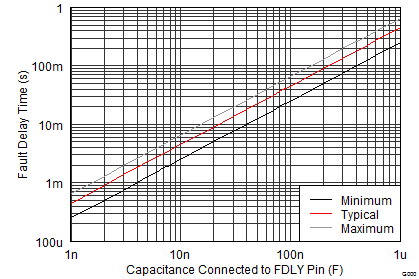 Figure 15. Adjustable Fault Delay Time
7.3.7.3 Thermal Shutdown
A thermal shutdown is implemented to prevent damage because of excessive heat and power dissipation. Typically, the thermal shutdown threshold is 155°C. When this threshold is reached, the device enters shutdown. The device can be enabled again by cycling the input supply voltage.
7.3.7.4 Undervoltage Lockout
The TPS65150-Q1 device has an undervoltage lockout (UVLO) function. The UVLO function stops device operation if the voltage on the VIN pin is less than the UVLO threshold voltage. This makes sure that the device only operates when the supply voltage is high enough for correct operation.
7.4 Device Functional Modes
Figure 16 shows the functional modes of the TPS65150-Q1.
7.4.1 VI > VIT+
When the input supply voltage is above the undervoltage lockout threshold, the device is on and all its functions are enabled. Note that full performance may not be available until the input supply voltage exceeds the minimum value specified in Recommended Operating Conditions.
7.4.2 VI < VIT–
When the input supply voltage is below the undervoltage lockout threshold, the TPS65150-Q1 device is off and all its functions are disabled.
7.4.3 Fault Mode
The TPS65150-Q1 device immediately enters fault mode when any of the following is detected:
- boost converter overvoltage
- overtemperature
The TPS65150-Q1 device also enters fault mode if any of the following conditions is detected and persists for longer than td(FDLY):
- boost converter output out of regulation
- negative charge pump output out of regulation
- positive charge pump output out of regulation
The TPS65150-Q1 device does not function during fault mode. Cycle the input supply voltage to exit fault mode and recover normal operation.
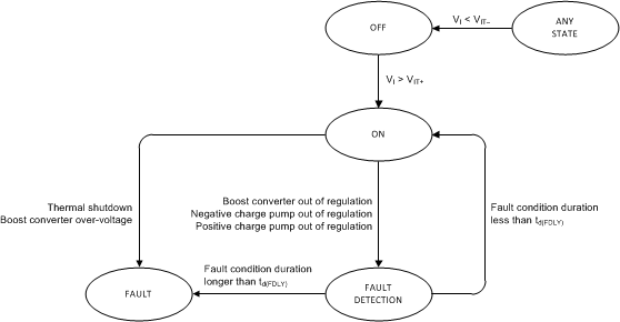 Figure 16. Functional Modes
