SLVSBX4C June 2013 – May 2017 TPS65150-Q1
PRODUCTION DATA.
- 1 Features
- 2 Applications
- 3 Description
- 4 Revision History
- 5 Pin Configuration and Functions
- 6 Specifications
- 7 Detailed Description
-
8 Application and Implementation
- 8.1 Application Information
- 8.2
Typical Application
- 8.2.1 Design Requirements
- 8.2.2
Detailed Design Procedure
- 8.2.2.1 Boost Converter Design Procedure
- 8.2.2.2 Rectifier Diode Selection
- 8.2.2.3 Setting the Output Voltage
- 8.2.2.4 Output Capacitor Selection
- 8.2.2.5 Input Capacitor Selection
- 8.2.2.6 Compensation
- 8.2.2.7 Negative Charge Pump
- 8.2.2.8 Positive Charge Pump
- 8.2.2.9 Gate Voltage Shaping
- 8.2.2.10 Power-On Sequencing
- 8.2.2.11 Fault Delay
- 8.2.3 Application Curves
- 8.3 System Examples
- 9 Power Supply Recommendations
- 10Layout
- 11Device and Documentation Support
- 12Mechanical, Packaging, and Orderable Information
Package Options
Mechanical Data (Package|Pins)
- PWP|24
Thermal pad, mechanical data (Package|Pins)
- PWP|24
Orderable Information
6 Specifications
6.1 Absolute Maximum Ratings
over operating free-air temperature range (unless otherwise noted)(1)(2)
(1) Stresses beyond those listed under Absolute Maximum Ratings may cause permanent damage to the device. These are stress ratings only, which do not imply functional operation of the device at these or any other conditions beyond those indicated under Recommended Operating Conditions. Exposure to absolute-maximum-rated conditions for extended periods may affect device reliability.
(2) All voltage values are with respect to network ground terminal.
6.2 ESD Ratings
| VALUE | UNIT | |||
|---|---|---|---|---|
| V(ESD) | Electrostatic discharge | Human-body model (HBM), per AEC-Q100-02 | ±2000 | V |
| Charged-device model (CDM), per AEC-Q100-011 | ±500 | |||
6.3 Recommended Operating Conditions
over operating free-air temperature range (unless otherwise noted)| MIN | NOM | MAX | UNIT | ||
|---|---|---|---|---|---|
| VI | Input voltage range | 1.8 | 6 | V | |
| V(VS) | Output voltage range of the boost converter V(VS) | 15 | V | ||
| L | Inductor(1) | 4.7 | µH | ||
| TA | Operating ambient temperature | –40 | 125 | °C | |
(1) See Typical Application for further information.
6.4 Thermal Information
| THERMAL METRIC(1) | TPS65150-Q1 | UNIT | |
|---|---|---|---|
| PWP (TSSOP) | |||
| 24 PINS | |||
| RθJA | Junction-to-ambient thermal resistance | 40.6 | °C/W |
| RθJC(top) | Junction-to-case (top) thermal resistance | 20.8 | °C/W |
| RθJB | Junction-to-board thermal resistance | 18.4 | °C/W |
| ψJT | Junction-to-top characterization parameter | 0.5 | °C/W |
| ψJB | Junction-to-board characterization parameter | 18.2 | °C/W |
| RθJC(bot) | Junction-to-case (bottom) thermal resistance | 1.9 | °C/W |
(1) For more information about traditional and new thermal metrics, see the Semiconductor and IC Package Thermal Metrics application report.
6.5 Electrical Characteristics
VI = 3.3 V, V(VS) = 10 V, TA = –40°C to 125°C, typical values are at TA = 25°C (unless otherwise noted)| PARAMETER | TEST CONDITIONS | MIN | TYP | MAX | UNIT | ||
|---|---|---|---|---|---|---|---|
| SUPPLY CURRENT | |||||||
| VI | Input voltage (VIN) | 1.8 | 6 | V | |||
| Supply current (VIN) | Device not switching | 14 | 25 | µA | |||
| Supply current (SUP) | Device not switching | 1.9 | 3 | mA | |||
| Supply current (VCOM buffer) | 750 | 1500 | µA | ||||
| VIT– | Undervoltage lockout threshold (VIN) | VI falling | –40 °C < TA < 85 °C | 1.6 | 1.8 | V | |
| –40 °C < TA < 125 °C | 1.6 | 1.85 | |||||
| VIT+ | Undervoltage lockout threshold (VIN) | VI rising | –40 °C < TA < 85 °C | 1.7 | 1.9 | V | |
| –40 °C < TA < 125 °C | 1.7 | 1.95 | |||||
| Thermal shutdown temperature threshold | TJ rising | 155 | °C | ||||
| Thermal shutdown temperature hysteresis | 10 | °C | |||||
| LOGIC SIGNALS | |||||||
| VIH | High-level input voltage (CTRL) | 1.6 | V | ||||
| VIL | Low-level input voltage (CTRL) | 0.4 | V | ||||
| IIH, IIL | Input current (CTRL) | CTRL = VI or GND | 0.01 | 0.2 | µA | ||
| BOOST CONVERTER | |||||||
| VO | Output voltage | 15 | V | ||||
| Vref | Boost converter reference voltage (FB) | –40 °C < TA < 85 °C | 1.136 | 1.146 | 1.154 | V | |
| –40 °C < TA < 125 °C | 1.132 | 1.146 | 1.160 | ||||
| IIB | Input bias current (FB) | 10 | 100 | nA | |||
| rDS(on) | Drain-source on-state resistance (Q1) | IDS = 500 mA | VO = 10 V | 200 | 300 | mΩ | |
| VO = 5 V | 305 | 450 | |||||
| rDS(on) | Drain-source on-state resistance (Q2) | IDS = 500 mA | VO = 10 V | 8 | 15 | Ω | |
| VO = 5 V | 12 | 22 | |||||
| IDS | Drain-source current rating (Q2) | 1 | A | ||||
| Current limit (Q1) | 2 | 2.5 | 3.4 | A | |||
| I(SW)(off) | Off-state current (SW) | V(SW) = 15 V | 1 | 10 | µA | ||
| VIT+ | Overvoltage protection threshold (SUP) | V(SUP) rising | 16 | 20 | V | ||
| ΔVO(ΔVI) | Line regulation | VI = 1.8 V to 5 V | IO = 1 mA | 0.007 | %/V | ||
| ΔVO(ΔIO) | Load regulation | VI = 5 V | IO = 0 A to 400 mA | 0.16 | %/A | ||
| VIT+ | Gate drive threshold (FB)(2) | –12% of Vref | –4% of Vref | V | |||
| NEGATIVE CHARGE PUMP | |||||||
| VO | Output voltage | –2 | V | ||||
| V(REF) | Reference output voltage (REF) | –40 °C < TA < 85 °C | 1.205 | 1.213 | 1.219 | V | |
| –40 °C < TA < 125 °C | 1.203 | 1.213 | 1.223 | ||||
| Vref | Feedback regulation voltage (FBN) | –36 | 0 | 36 | mV | ||
| IIB | Input bias current (FBN) | 10 | 100 | nA | |||
| rDS(on) | Drain-source on-state resistance (Q4) | IDS = 20 mA | 4.4 | Ω | |||
| V(DRVN) | Current sink voltage drop(1) | V(FBN) = 5% above nominal voltage | I(DRVN) = 50 mA | 130 | 300 | mV | |
| I(DRVN) = 100 mA | 280 | 450 | |||||
| ΔVO(ΔIO) | Load regulation | VO = –5 V | IO = 0 mA to 20 mA | 0.016 | %/mA | ||
| POSITIVE CHARGE PUMP | |||||||
| VO | Output voltage | CTRL = GND | VGH = open | 30 | V | ||
| Vref | Feedback regulation voltage (FBP) | CTRL = GND | VGH = open | 1.187 | 1.214 | 1.238 | V |
| IIB | Input bias current (FBP) | CTRL = GND | VGH = open | 10 | 100 | nA | |
| rDS(on) | Drain-source on-state resistance (Q3) | IDS = 20 mA | 1.1 | Ω | |||
| V(SUP) – V(DRVP) | Current sink voltage drop(1) | V(FBP) = 5% below nominal voltage | I(DRVP) = 50 mA | 420 | 650 | mV | |
| I(DRVP)= 100 mA | 900 | 1400 | |||||
| ΔVO(ΔIO) | Load regulation | VO = 24 V | IO = 0 mA to 20 mA | 0.07 | %/mA | ||
| GATE-VOLTAGE SHAPING | |||||||
| rDS(on) | Drain-source on-state resistance (Q5) | IO = –20 mA | 12 | 30 | Ω | ||
| I(ADJ) | Capacitor charge current | V(ADJ) = 20 V | V(CPI) = 30 V | 160 | 200 | 240 | µA |
| VOmin | Minimum output voltage | V(ADJ) = 0 V | IO = –10 mA | 2 | V | ||
| IOM | Maximum output current | 20 | mA | ||||
| TIMING CIRCUITS DLY1, DLY2, FDLY | |||||||
| I(DLY1) | Drive current into delay capacitor (DLY1) | V(DLY1) = 1.213 V | 3 | 5 | 7 | µA | |
| I(DLY2) | Drive current into delay capacitor (DLY2) | V(DLY2) = 1.213 V | 3 | 5 | 7 | µA | |
| R(FDLY) | Fault time delay resistor | 250 | 450 | 650 | kΩ | ||
| GATE DRIVE (GD) | |||||||
| V(GD_VS) | Gate Drive Threshold | V(VS) rising | –12% of V(SUP) | –4% of V(SUP) | |||
| VOL | Low-level output voltage (GD) | IOL = 500 µA | 0.5 | V | |||
| IOH | Off-state current (GD) | VOH = 15 V | 0.001 | 1 | µA | ||
| VCOM BUFFER | |||||||
| VISR | Single-ended input voltage (IN) | 2.25 | V(SUP) – 2 V | V | |||
| VIO | Input offset voltage (IN) | IO = 0 mA | –25 | 25 | mV | ||
| ΔVO(ΔIO) | Load regulation | IO = ±25 mA | –37 | 37 | mV | ||
| IO = ±50 mA | –77 | 55 | |||||
| IO = ±100 mA | –85 | 85 | |||||
| IO = ±150 mA | –110 | 110 | |||||
| IIB | Input bias current (IN) | –300 | –30 | 300 | nA | ||
| IOM | Maximum output current (VCOM) | V(SUP) = 15 V | 1.2 | A | |||
| V(SUP) = 10 V | 0.65 | ||||||
| V(SUP) = 5 V | 0.15 | ||||||
(1) The maximum charge pump output current is half the drive current of the internal current source or sink.
(2) The GD signal is latched low when the main boost converter output is within regulation. The GD signal is reset when the voltage on the VIN pin goes below the UVLO threshold voltage.
6.6 Switching Characteristics
over operating free-air temperature range (unless otherwise noted)| PARAMETER | TEST CONDITIONS | MIN | TYP | MAX | UNIT | |
|---|---|---|---|---|---|---|
| Oscillator frequency | 1.02 | 1.2 | 1.38 | MHz | ||
| Duty cycle (DRVN) | 50% | |||||
| Duty cycle (DRVP) | 50% | |||||
6.7 Typical Characteristics
The typical characteristics are measured at 3.3 VTable 1. Table Of Graphs
| FIGURE | |||
|---|---|---|---|
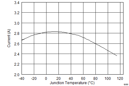
| Boost converter switch (Q1) current limit | vs temperature | Figure 1 | |
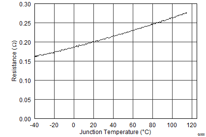
| Boost converter switch (Q1) rDS(on) | vs temperature | Figure 2 | |
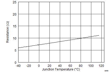
| Boost converter rectifier (Q2) rDS(on) | vs temperature | Figure 3 | |
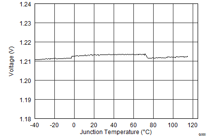
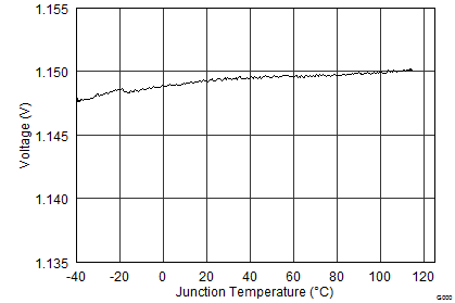
| Boost converter reference Voltage | vs temperature | Figure 4 | |
| Positive charge pump reference voltage | vs temperature | Figure 5 | |
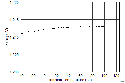
| REF pin voltage | vs temperature | Figure 6 | |
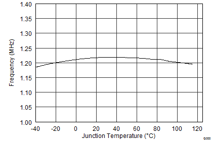
| Oscillator frequency | vs temperature | Figure 7 | |
