SLVSAA2D March 2010 – January 2016 TPS65182 , TPS65182B
PRODUCTION DATA.
- 1 Features
- 2 Applications
- 3 Description
- 4 Revision History
- 5 Pin Configuration and Functions
- 6 Specifications
-
7 Detailed Description
- 7.1 Overview
- 7.2 Functional Block Diagram
- 7.3
Feature Description
- 7.3.1 Modes of Operation
- 7.3.2 Mode Transistions
- 7.3.3 Wake-Up and Power Up Sequencing
- 7.3.4 Dependencies Between Rails
- 7.3.5 Soft-Start
- 7.3.6 VCOM Adjustment
- 7.3.7 VPOS and VNEG Supply Tracking
- 7.3.8 Fault Handling and Recovery
- 7.3.9 Power Good Pin
- 7.3.10 Panel Temperature Monitoring
- 7.3.11 NTC Bias Circuit
- 7.4 Device Functional Modes
- 7.5 Register Maps
- 8 Application and Implementation
- 9 Power Supply Recommendations
- 10Layout
- 11Device and Documentation Support
- 12Mechanical, Packaging, and Orderable Information
Package Options
Mechanical Data (Package|Pins)
- RGZ|48
Thermal pad, mechanical data (Package|Pins)
- RGZ|48
Orderable Information
10 Layout
10.1 Layout Guidelines
The layout guidelines for TPS65182x are as follows:
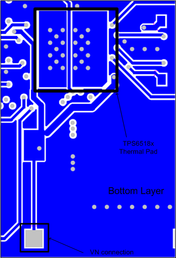
- PBKG (Die substrate must connect to VN (–16 V) with short, wide trace. Wide copper trace will improve heat dissipation.
- Power pad is internally connected to PBKG and must be connected to ground, but connected to VN with a short wide copper trace.
- Inductor traces must be kept on the PCB top layer free of any vias.
- Feedback traces must be routed away from any potential noise source to avoid coupling.
- Output caps must be placed immediately at output pin.
- VIN pins must be bypassed to ground with low ESR ceramic bypass capacitors.
10.2 Layout Example
 Figure 14. Typical Layout of TPS6518x