SLVSAA2D March 2010 – January 2016 TPS65182 , TPS65182B
PRODUCTION DATA.
- 1 Features
- 2 Applications
- 3 Description
- 4 Revision History
- 5 Pin Configuration and Functions
- 6 Specifications
-
7 Detailed Description
- 7.1 Overview
- 7.2 Functional Block Diagram
- 7.3
Feature Description
- 7.3.1 Modes of Operation
- 7.3.2 Mode Transistions
- 7.3.3 Wake-Up and Power Up Sequencing
- 7.3.4 Dependencies Between Rails
- 7.3.5 Soft-Start
- 7.3.6 VCOM Adjustment
- 7.3.7 VPOS and VNEG Supply Tracking
- 7.3.8 Fault Handling and Recovery
- 7.3.9 Power Good Pin
- 7.3.10 Panel Temperature Monitoring
- 7.3.11 NTC Bias Circuit
- 7.4 Device Functional Modes
- 7.5 Register Maps
- 8 Application and Implementation
- 9 Power Supply Recommendations
- 10Layout
- 11Device and Documentation Support
- 12Mechanical, Packaging, and Orderable Information
Package Options
Mechanical Data (Package|Pins)
- RGZ|48
Thermal pad, mechanical data (Package|Pins)
- RGZ|48
Orderable Information
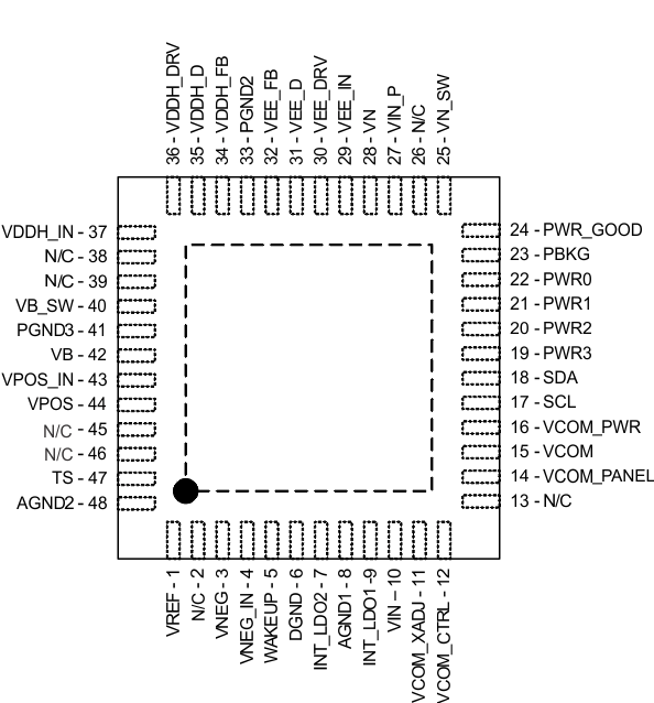
5 Pin Configuration and Functions
RGZ Package
48-Pin VQFN With Exposed Thermal Pad
Top View

Pin Functions
| PIN | I/O | DESCRIPTION(1) | |
|---|---|---|---|
| NO. | NAME | ||
| 1 | VREF | O | Filter pin for 2.25-V internal reference to ADC |
| 2 | N/C | — | Not connected |
| 3 | VNEG | O | Negative supply output pin for panel source drivers |
| 4 | VNEG_IN | I | Input pin for LDO2 (VNEG) |
| 5 | WAKEUP | I | Wake up pin (active high). Pull this pin high to wake up from sleep mode. |
| 6 | DGND | — | Digital ground |
| 7 | INT_LDO2 | O | Internal supply (digital circuitry) filter pin |
| 8 | AGND1 | — | Analog ground for general analog circuitry |
| 9 | INT_LDO1 | O | Internal supply (analog circuitry) filter pin |
| 10 | VIN | I | Input power supply to general circuitry |
| 11 | VCOM_XADJ | I | Analog input for conventional VCOM setup method. Tie this pin to ground if VCOM is set through I2C interface. |
| 12 | VCOM_CTRL | I | VCOM_PANEL gate driver enable (active high) |
| 13 | N/C | — | Not connected |
| 14 | VCOM_PANEL | O | Panel common-voltage output pin |
| 15 | VCOM | O | Filter pin for panel common-voltage driver |
| 16 | VCOM_PWR | I | Internal supply input pin to VCOM buffer. Connect to the output of DCDC2. |
| 17 | SCL | I | Serial interface (I2C) clock input |
| 18 | SDA | I/O | Serial interface (I2C) data input/output |
| 19 | PWR3 | I | Enable pin for CP1 (VDDH) (active high) |
| 20 | PWR2 | I | Enable pin for LDO1 (VPOS) (active high) |
| 21 | PWR1 | I | Enable pin for CP2 (VEE) (active high) |
| 22 | PWR0 | I | Enable pin for LDO2 (VNEG) and VCOM (active high) |
| 24 | PWR_GOOD | O | Open drain power good output pin (active low) |
| 25 | VN_SW | O | Inverting buck-boost converter switch out (DCDC2) |
| 26 | N/C | — | Not connected |
| 27 | VIN_P | I | Input power supply to inverting buck-boost converter (DCDC2) |
| 28 | VN | I | Feedback pin for inverting buck-boost converter (DCDC2) |
| 29 | VEE_IN | I | Input supply pin for CP1 (VEE) |
| 30 | VEE_DRV | O | Driver output pin for negative charge pump (CP2) |
| 31 | VEE_D | O | Base voltage output pin for negative charge pump (CP2) |
| 32 | VEE_FB | I | Feedback pin for negative charge pump (CP2) |
| 33 | PGND2 | — | Power ground for CP1 (VDDH) and CP2 (VEE) charge pumps |
| 34 | VDDH_FB | I | Feedback pin for positive charge pump (CP1) |
| 35 | VDDH_D | O | Base voltage output pin for positive charge pump (CP1) |
| 36 | VDDH_DRV | O | Driver output pin for positive charge pump (CP1) |
| 37 | VDDH_IN | I | Input supply pin for positive charge pump (CP1) |
| 38 | N/C | — | Not connected |
| 39 | N/C | — | Not connected |
| 40 | VB_SW | O | Boost converter switch out (DCDC1) |
| 41 | PGND3 | — | Power ground for DCDC1 |
| 42 | VB | I | Feedback pin for boost converter (DCDC1) |
| 43 | VPOS_IN | I | Input pin for LDO1 (VPOS) |
| 44 | VPOS | O | Positive supply output pin for panel source drivers |
| 45 | N/C | — | Not connected |
| 46 | N/C | — | Not connected |
| 47 | TS | I | Thermistor input pin. Connect a 10k NTC thermistor and a 43k linearization resistor between this pin and AGND2. |
| 48 | AGND2 | — | Reference point to external thermistor and linearization resistor |
| 23 | PowerPad (PBKG) | — | Die substrate/thermal pad. Connect to VN with short, wide trace. Wide copper trace will improve heat dissipation. PowerPad must not be connected to ground. |
(1) There will be 0-ns, 93.75-µs, 62.52-µs of deglitch for PWRx, WAKEUP, and VCOM_CTRL, respectively.