SLVSD87C december 2015 – may 2023 TPS65262-2
PRODUCTION DATA
- 1
- 1 Features
- 2 Applications
- 3 Description
- 4 Revision History
- 5 Pin Configuration and Functions
- 6 Specifications
-
7 Detailed Description
- 7.1 Overview
- 7.2 Functional Block Diagram
- 7.3
Feature Description
- 7.3.1 Adjusting the Output Voltage
- 7.3.2 Enable and Adjusting Undervoltage Lockout
- 7.3.3 Soft-Start Time
- 7.3.4 Power-Up Sequencing
- 7.3.5 V7V Low Dropout Regulator and Bootstrap
- 7.3.6 Out-of-Phase Operation
- 7.3.7 Output Overvoltage Protection (OVP)
- 7.3.8 PSM
- 7.3.9 Slope Compensation
- 7.3.10 Overcurrent Protection
- 7.3.11 Power Good
- 7.3.12 Thermal Shutdown
- 7.4 Device Functional Modes
- 8 Application and Implementation
- 9 Device and Documentation Support
- 10Mechanical, Packaging, and Orderable Information
Package Options
Mechanical Data (Package|Pins)
- RHB|32
Thermal pad, mechanical data (Package|Pins)
- RHB|32
Orderable Information
3 Description
The TPS65262-2 is a monolithic, triple, synchronous step-down (buck) converter with 3-A/1-A/1-A output current. A wide 4.5-V to 18-V input supply voltage range encompasses the most intermediate bus voltage operating off 5-V, 9-V, 12-V, or 15-V power bus. The converter, with constant frequency peak current mode, is designed to simplify its application while giving designers options to optimize the system according to targeted applications. The device operates at 600-kHz fixed switching frequency. The loop compensations for buck2 and buck3 have been integrated for less external components. The 180° out-of-phase operation between buck1 and buck2, 3 (buck2 and buck3 run in phase) minimizes the input filter requirements.
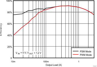
The TPS65262-2 operates in pulse skipping mode (PSM) with connecting MODE pin to GND and operates in force continuous current mode (FCC) with driving MODE pin to high or leaving float. PSM mode provides high efficiency by reducing switching losses at light load and FCC mode reduces noise susceptibility and RF interference.
Two low dropout voltage linear regulators (LDO) are also built in TPS65262-2 with input voltage range 1.3 V to 18 V, continuous output current 350 mA/150 mA, independent enable and adjustable output voltage.
A power-good pin asserts when any output voltages are out of regulation.
| PART NUMBER | PACKAGE | BODY SIZE (NOM) |
|---|---|---|
| TPS65262-2 | RHB (VQFN, 32) | 5.00 mm × 5.00 mm |
 Application Schematic
 Efficiency vs Output
Load