SLVS979C October 2009 – May 2018 TPS65720 , TPS65721
PRODUCTION DATA.
- 1 Features
- 2 Applications
- 3 Description
- 4 Revision History
- 5 Device Options
- 6 Pin Configuration and Functions
- 7 Specifications
-
8 Detailed Description
- 8.1 Overview
- 8.2 Functional Block Diagrams
- 8.3
Feature Description
- 8.3.1 Battery Charger and Power Path
- 8.3.2 Power-Path Management
- 8.3.3 Battery Charging
- 8.3.4 Thermal Regulation and Thermal Shutdown
- 8.3.5 Battery Pack Temperature Monitoring
- 8.3.6 DCDC1 Converter
- 8.3.7 Power Save Mode
- 8.3.8 Short-Circuit Protection
- 8.3.9 Thermal Shutdown
- 8.3.10 LDO1
- 8.4 Device Functional Modes
- 8.5 Programming
- 8.6
Register Maps
- 8.6.1 CHGSTATUS Register Address: 01h (read only)
- 8.6.2 CHGCONFIG0 Register Address: 02h (read/write)
- 8.6.3 CHGCONFIG1 Register Address: 03h (read/write)
- 8.6.4 CHGCONFIG2 Register Address: 04h (read/write)
- 8.6.5 CHGCONFIG3 Register Address: 05h (read/write)
- 8.6.6 CHGSTATE Register Address: 06h (read only)
- 8.6.7 DEFDCDC1 Register Address: 07h (read/write)
- 8.6.8 LDO_CTRL Register Address: 08h (read/write)
- 8.6.9 CONTROL0 Register Address: 09h (read/write)
- 8.6.10 CONTROL1 Register Address: 0Ah (read/write)
- 8.6.11 GPIO_SSC Register Address: 0Bh (read/write)
- 8.6.12 GPIODIR Register Address: 0Ch (read/write)
- 8.6.13 IRMASK0 Register Address: 0Dh (read/write)
- 8.6.14 IRMASK1 Register Address: 0Eh (read/write)
- 8.6.15 IRMASK2 Register Address: 0Fh (read/write)
- 8.6.16 IR0 Register Address: 10h (read only)
- 8.6.17 IR1 Register Address: 11h (read)
- 8.6.18 IR2 Register Address: 12h (read)
- 9 Application and Implementation
- 10Power Supply Recommendations
- 11Layout
- 12Device and Documentation Support
- 13Mechanical, Packaging, and Orderable Information
Package Options
Mechanical Data (Package|Pins)
- RSN|32
Thermal pad, mechanical data (Package|Pins)
- RSN|32
Orderable Information
3 Description
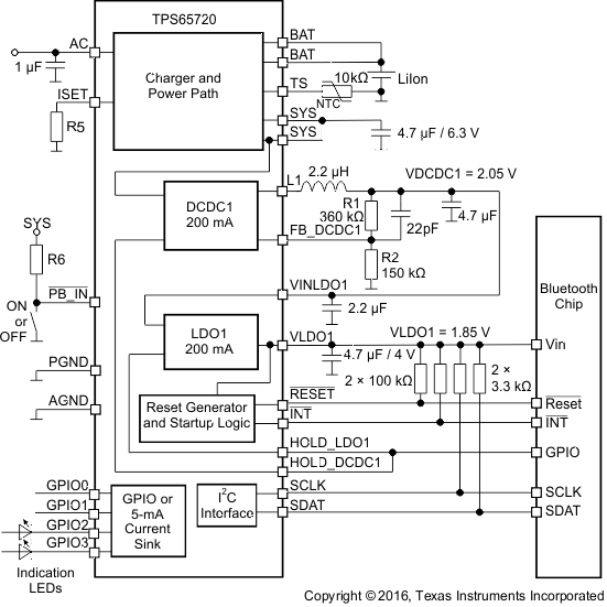
The TPS6572x device is a small power management unit targeted for Bluetooth headsets or other portable low-power consumer-end equipments. The device contains an USB friendly Lithium-Ion battery charger, a highly efficient step-down converter, a low-dropout linear regulator, and additional supporting functions. The device is controlled by an I2C interface. Several settings can be customized by the use of nonvolatile memory which is factory programmed.
The 2.25-MHz step-down converter enters a low-power mode at light load for maximum efficiency across the widest possible range of load currents. For low-noise applications the devices can be forced into fixed-frequency PWM mode using the I2C-compatible interface.
The device allows the use of small inductors and capacitors to achieve a small solution size. The TPS65720 provides an output current of up to
200 mA on the DC-DC converter while TPS657201, TPS657202, and TPS65721 provide up to 400 mA. The TPS6572x also integrates one 200-mA LDO. The LDO operates with an input voltage range from 1.8 V to 5.6 V, thus allowing it to be supplied from the output of the step-down converter or directly from the system voltage.
The TPS65720, TPS657201, and TPS657202 come in a small 25-ball 2-mm × 2-mm wafer chip scale package (DSBGA) with 0.4-mm ball pitch or a
4-mm × 4-mm WQFN package with a 0.4-mm pitch (TPS65721).
Device Information (1)
| PART NUMBER | PACKAGE | BODY SIZE (NOM) |
|---|---|---|
| TPS65720x | DSBGA (25) | 2.11 mm × 2.11 mm |
| TPS65721 | WQFN (32) | 4.00 mm × 4.00 mm |
- For all available packages, see the orderable addendum at the end of the data sheet.
Typical Application Schematic
