SLVS979C October 2009 – May 2018 TPS65720 , TPS65721
PRODUCTION DATA.
- 1 Features
- 2 Applications
- 3 Description
- 4 Revision History
- 5 Device Options
- 6 Pin Configuration and Functions
- 7 Specifications
-
8 Detailed Description
- 8.1 Overview
- 8.2 Functional Block Diagrams
- 8.3
Feature Description
- 8.3.1 Battery Charger and Power Path
- 8.3.2 Power-Path Management
- 8.3.3 Battery Charging
- 8.3.4 Thermal Regulation and Thermal Shutdown
- 8.3.5 Battery Pack Temperature Monitoring
- 8.3.6 DCDC1 Converter
- 8.3.7 Power Save Mode
- 8.3.8 Short-Circuit Protection
- 8.3.9 Thermal Shutdown
- 8.3.10 LDO1
- 8.4 Device Functional Modes
- 8.5 Programming
- 8.6
Register Maps
- 8.6.1 CHGSTATUS Register Address: 01h (read only)
- 8.6.2 CHGCONFIG0 Register Address: 02h (read/write)
- 8.6.3 CHGCONFIG1 Register Address: 03h (read/write)
- 8.6.4 CHGCONFIG2 Register Address: 04h (read/write)
- 8.6.5 CHGCONFIG3 Register Address: 05h (read/write)
- 8.6.6 CHGSTATE Register Address: 06h (read only)
- 8.6.7 DEFDCDC1 Register Address: 07h (read/write)
- 8.6.8 LDO_CTRL Register Address: 08h (read/write)
- 8.6.9 CONTROL0 Register Address: 09h (read/write)
- 8.6.10 CONTROL1 Register Address: 0Ah (read/write)
- 8.6.11 GPIO_SSC Register Address: 0Bh (read/write)
- 8.6.12 GPIODIR Register Address: 0Ch (read/write)
- 8.6.13 IRMASK0 Register Address: 0Dh (read/write)
- 8.6.14 IRMASK1 Register Address: 0Eh (read/write)
- 8.6.15 IRMASK2 Register Address: 0Fh (read/write)
- 8.6.16 IR0 Register Address: 10h (read only)
- 8.6.17 IR1 Register Address: 11h (read)
- 8.6.18 IR2 Register Address: 12h (read)
- 9 Application and Implementation
- 10Power Supply Recommendations
- 11Layout
- 12Device and Documentation Support
- 13Mechanical, Packaging, and Orderable Information
Package Options
Mechanical Data (Package|Pins)
- RSN|32
Thermal pad, mechanical data (Package|Pins)
- RSN|32
Orderable Information
6 Pin Configuration and Functions
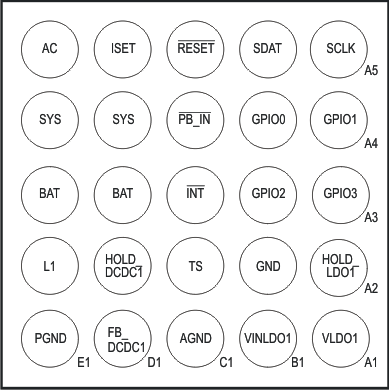
YFF Package
25-Pin DSBGA
Bottom View

Pin Functions—DSBGA (TPS65720)
| PIN | I/O | DESCRIPTION | |
|---|---|---|---|
| NO. | NAME | ||
| A1 | VLDO1 | O | Output voltage of LDO1 |
| A2 | HOLD_LDO1 | I | Power-on input for LDO1. When pulled HIGH, LDO1 is kept enabled after PB_IN was released HIGH. |
| A3 | GPIO3 | I/O | General purpose I/O or 5-mA current sink |
| A4 | GPIO1 | I/O | General purpose I/O |
| A5 | SCLK | I | Clock input for the I2C interface |
| B1 | VINLDO1 | I | Input voltage for LDO1 |
| B2 | GND | — | Connect to AGND and PGND |
| B3 | GPIO2 | I/O | General purpose I/O or 5-mA current sink |
| B4 | GPIO0 | I/O | General purpose I/O |
| B5 | SDAT | I/O | Data line for the I2C interface |
| C1 | AGND | — | Analog ground |
| C2 | TS | I | Connect a thermistor from this pin to GND for battery temperature |
| C3 | INT | O | Open-drain interrupt output |
| C4 | PB_IN | I | Push button input; Turns on DCDC1 and LDO1 if pulled to GND. |
| C5 | RESET | O | Open-drain output of the reset generator; This output goes active LOW when the output voltage of LDO1 falls 8% below its target voltage. |
| D1 | FB_DCDC1 | I | Feedback input of step-down converter |
| D2 | HOLD_DCDC1 | I | Power-On input for DCDC1 converter. When pulled HIGH, the DC-DC converter is kept enabled after PB_IN was released HIGH. |
| D3 | BAT | I/O | Connect to battery + terminal |
| D4 | SYS | O | System voltage; output of the power path manager. Power input for step-down converter DCDC1 |
| D5 | ISET | I | Connect a resistor from this pin to GND to set fast charge current |
| E1 | PGND | — | Power ground |
| E2 | L1 | O | Switch output of step-down converter |
| E3 | BAT | I/O | Connect to battery + terminal |
| E4 | SYS | O | System voltage; output of the power path manager. Power input for step-down converter DCDC1 |
| E5 | AC | I | Input power for power manager, connect to external DC supply. |
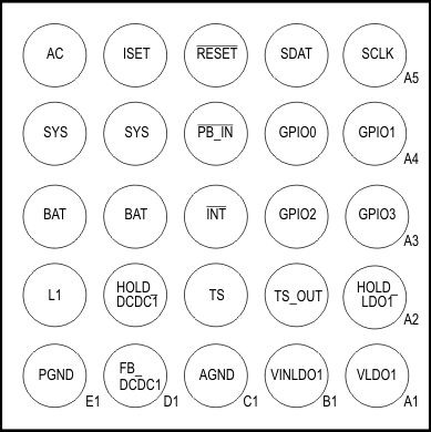
YFF Package
25-Pin DSBGA
Bottom View

Pin Functions—DSBGA (TPS657201, TPS657202)
| PIN | I/O | DESCRIPTION | |
|---|---|---|---|
| NO. | NAME | ||
| A1 | VLDO1 | O | Output voltage of LDO1 |
| A2 | HOLD_LDO1 | I | Power-on input for LDO1. When pulled HIGH, LDO1 is kept enabled after PB_IN was released HIGH. |
| A3 | GPIO3 | I/O | General purpose I/O or 5-mA current sink |
| A4 | GPIO1 | I/O | General purpose I/O |
| A5 | SCLK | I | Clock input for the I2C interface |
| B1 | VINLDO1 | I | Input voltage for LDO1 |
| B2 | VBAT/TS_OUT | O | Output of battery temperature and battery voltage monitor |
| B3 | GPIO2 | I/O | General purpose I/O or 5-mA current sink |
| B4 | GPIO0 | I/O | General purpose I/O |
| B5 | SDAT | I/O | Data line for the I2C interface |
| C1 | AGND | — | Analog ground |
| C2 | TS | I | Connect a thermistor from this pin to GND for battery temperature |
| C3 | INT | O | Open-drain interrupt output |
| C4 | PB_IN | I | Push button input; Turns on DCDC1 and LDO1 if pulled to GND. |
| C5 | RESET | O | Open-drain output of the reset generator; This output goes active LOW when the output voltage of LDO1 falls 8% below its target voltage. |
| D1 | FB_DCDC1 | I | Feedback input of step-down converter |
| D2 | HOLD_DCDC1 | I | Power-on input for DCDC1 converter. When pulled HIGH, the DC-DC converter is kept enabled after PB_IN was released HIGH. |
| D3 | BAT | I/O | Connect to battery + terminal |
| D4 | SYS | O | System voltage; output of the power path manager. Power input for step-down converter DCDC1 |
| D5 | ISET | I | Connect a resistor from this pin to GND to set fast charge current |
| E1 | PGND | — | Power ground |
| E2 | L1 | O | Switch output of step-down converter |
| E3 | BAT | I/O | Connect to battery + terminal |
| E4 | SYS | O | System voltage; output of the power path manager. Power input for step-down converter DCDC1 |
| E5 | AC | I | Input power for power manager, connect to external DC supply. |
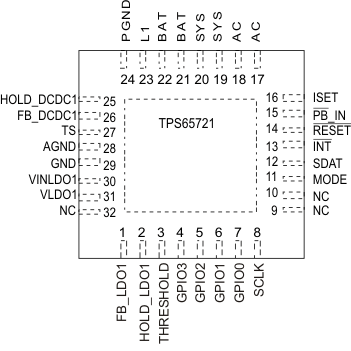
RSN Package
32-Pin WQFN With Thermal Pad
Top View

Pin Functions—WQFN (TPS65721)
| PIN | I/O | DESCRIPTION | |
|---|---|---|---|
| NAME | NO. | ||
| AC | 17, 18 | I | Input power for power manager, connect to external DC supply. |
| AGND | 28 | — | Analog ground |
| BAT | 21, 22 | I/O | Connect to battery + terminal |
| FB_DCDC1 | 26 | I | Feedback input of step-down converter |
| FB_LDO1 | 1 | I | Feedback input for LDO1 |
| GND | 29 | — | Connect to AGND and PGND |
| GPIO0 | 7 | I/O | General purpose I/O |
| GPIO1 | 6 | I/O | General purpose I/O |
| GPIO2 | 5 | I/O | General purpose I/O or 5-mA current source |
| GPIO3 | 4 | I/O | General purpose I/O or 5-mA current source |
| HOLD_DCDC1 | 25 | I | Power-on input for DCDC1 converter. When pulled HIGH, the DC-DC converter is kept enabled after PB_IN was released HIGH. |
| HOLD_LDO1 | 2 | I | Power-on input for LDO1. When pulled HIGH, LDO1 is kept enabled after PB_IN was released HIGH. |
| INT | 13 | O | Open-drain interrupt output |
| ISET | 16 | I | Connect a resistor from this pin to GND to set fast charge current |
| L1 | 23 | O | Switch output of step-down converter |
| MODE | 11 | I | Pull HIGH to force the DCDC1 converter to PWM mode. |
| PB_IN | 15 | I | Push button input; Turns on DCDC1 and LDO1 if pulled to GND. |
| PGND | 24 | — | Power ground |
| RESET | 14 | O | Open-drain output of the reset generator; This output goes active LOW when the input voltage at pin THRESHOLD falls below the threshold voltage. |
| SCLK | 8 | I | Clock input for the I2C interface |
| SDAT | 12 | I/O | Data line for the I2C interface |
| SYS | 19, 20 | O | System voltage; output of the power path manager. Power input for step-down converter DCDC1 |
| THRESHOLD | 3 | I | Input voltage to the reset comparator. When the input voltage falls below the threshold, the RESET output is actively pulled LOW. |
| TS | 27 | I | Connect a thermistor from this pin to GND for battery temperature |
| VINLDO1 | 30 | I | Input voltage for LDO1 |
| VLDO1 | 31 | O | Output voltage from LDO1 |
| ThermalPad | — | — | Connect to GND |