SLVSEW8B August 2019 – December 2019 TPS66020 , TPS66021
PRODUCTION DATA.
- 1 Features
- 2 Applications
- 3 Description
- 4 Revision History
- 5 Pin Configuration and Functions
-
6 Specifications
- 6.1 Absolute Maximum Ratings
- 6.2 ESD Ratings
- 6.3 Recommended Operating Conditions
- 6.4 Recommended Supply Load Capacitance
- 6.5 Thermal Information
- 6.6 PP5V Power Switch Characteristics
- 6.7 PPHV Power Switch Characteristics
- 6.8 Power Path Supervisory
- 6.9 VBUS LDO Characteristics
- 6.10 Thermal Shutdown Characteristics
- 6.11 Input-output (I/O) Characteristics
- 6.12 Power Consumption Characteristics
- 6.13 Typical Characteristics
- 7 Parameter Measurement Information
-
8 Detailed Description
- 8.1 Overview
- 8.2 Functional Block Diagram
- 8.3 Feature Description
- 8.4 Device Functional Modes
-
9 Application and Implementation
- 9.1 Application Information
- 9.2
Typical Application
- 9.2.1 Design Requirements
- 9.2.2
Detailed Design Procedure
- 9.2.2.1 External Current Reference Resistor (RIREF)
- 9.2.2.2 External VLDO Capacitor (CVLDO)
- 9.2.2.3 PP5V Power Path Capacitance
- 9.2.2.4 PPHV, VBUS Power Path Capacitance
- 9.2.2.5 VBUS TVS Protection (Optional)
- 9.2.2.6 VBUS Schottky Diode Protection (Optional)
- 9.2.2.7 VBUS Overvoltage Protection (Optional)
- 9.2.2.8 Dead Battery Support
- 9.2.2.9 Fast Role Swap (FRS) (Optional)
- 9.2.3 Application Curves
- 10Power Supply Recommendations
- 11Layout
- 12Device and Documentation Support
- 13Mechanical, Packaging, and Orderable Information
Package Options
Mechanical Data (Package|Pins)
- YBG|28
Thermal pad, mechanical data (Package|Pins)
Orderable Information
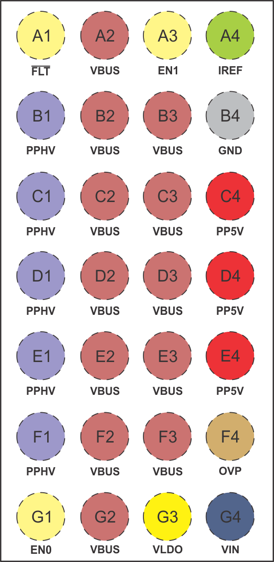
5 Pin Configuration and Functions
TPS6602x YBG Package
28-Pin WCSP
Top View

Pin Functions
| Pin | I/O | Reset State | Description | |
|---|---|---|---|---|
| Name | No. | |||
| PP5V | C4, D4, E4 | Power | Off | 5-V System Supply to VBUS. Bypass with capacitance CPP5V to GND. |
| PPHV | B1, C1, D1, E1, F1 | Power | Off | HV System Supply from VBUS. Bypass with capacitance CPPHV to GND. |
| VBUS | A2, B2, B3, C2, C3, D2, D3, E2, E3, F2, F3, G2 | Power | - | 5-V to 20-V nominal input supply to PPHV or 5-V output supply from PP5V. Bypass with capacitance CVBUS to GND. |
| VIN | G4 | Power | - | Device input supply. Bypass with capacitance CVIN to GND. |
| VLDO | G3 | Power | - | VIN supply or VBUS LDO regulated supply output from power multipexer. Bypass with capacitance CVLDO to GND. |
| GND | B4 | Ground | - | Ground. Connect all pins to ground plane. |
| OVP | F4 | Analog | - | Selects VBUS OVP. Tie pin to VBUS resistor divider output to set desired VBUS OVP level. Tie pin to GND to remove VBUS OVP function. |
| EN1 | A3 | Digital Input | Pull-down | Enable control signal for PPHV Sink and PP5V Source paths. Internal pull-down. |
| EN0 | G1 | Digital Input | Pull-down | Enable control signal for PPHV Sink and PP5V Source paths. Internal pull-down. |
| IREF | A4 | Analog | Used to set the PP5V source path current limit bias using an external resistor tied to GND. | |
| FLT | A1 | Digital Output | Hi-Z | Fault Output Indicator. Active low. This pin is a true open-drain (no PMOS). Float pin when unused. |