SBVS355C June 2019 – May 2022 TPS745-Q1
PRODUCTION DATA
- 1 Features
- 2 Applications
- 3 Description
- 4 Revision History
- 5 Pin Configuration and Functions
- 6 Specifications
- 7 Detailed Description
- 8 Application and Implementation
- 9 Power Supply Recommendations
- 10Layout
- 11Device and Documentation Support
- 12Mechanical, Packaging, and Orderable Information
Package Options
Mechanical Data (Package|Pins)
Thermal pad, mechanical data (Package|Pins)
Orderable Information
3 Description
The TPS745-Q1 is a 500-mA ultra-low-dropout regulator (LDO) with power-good functionality. This device is available in a small 6-pin, 2-mm × 2-mm WSON package and a small 8-pin, 3-mm × 3-mm VSON package with wettable flanks to facilitate optical inspection. The TPS745-Q1 consumes low quiescent current and provides fast line and load transient performance.
The TPS745-Q1 is a flexible device for post-regulation by supporting an input voltage range from 1.5 V to 6.0 V and an externally adjustable output range of 0.55 V to 5.5 V. The device also features fixed output voltages for powering common voltage rails.
The TPS745-Q1 has a power-good (PG) output that monitors the voltage at the feedback pin to indicate the status of the output voltage. The EN input and PG output can be used for sequencing multiple power supplies in the system.
The TPS745-Q1 is stable with small ceramic output capacitors, allowing for a small overall solution size. A precision band-gap and error amplifier provides high accuracy of ±0.85% (max) at 25°C and ±1.5% (max) over temperature. This device includes integrated thermal shutdown, current limit, and undervoltage lockout (UVLO) features. The TPS745-Q1 has an internal foldback current limit that helps reduce the thermal dissipation during short-circuit events.
| PART NUMBER | PACKAGE | BODY SIZE (NOM) |
|---|---|---|
| TPS745-Q1 | Wettable flank WSON (6) | 2.00 mm × 2.00 mm |
| Wettable flank VSON (8) | 3.00 mm × 3.00 mm |
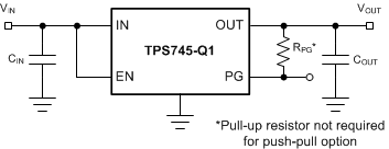
 Typical Application: Fixed Voltage Version
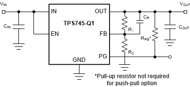
 Typical Application: Adjustable Voltage Version