SBVS074M january 2007 – april 2023
PRODUCTION DATA
- 1 Features
- 2 Applications
- 3 Description
- 4 Revision History
- 5 Pin Configuration and Functions
-
6 Specifications
- 6.1 Absolute Maximum Ratings
- 6.2 ESD Ratings
- 6.3 Recommended Operating Conditions
- 6.4 Thermal Information
- 6.5 Electrical Characteristics: Other Orderable Devices (non-M3 Suffix)
- 6.6 Electrical Characteristics: Orderable Device with M3 suffix
- 6.7 Typical Characteristics: IOUT = 50 mA
- 6.8 Typical Characteristics: IOUT = 1 A
- 6.9 Typical Characteristics: IOUT = 50 mA (M3 Suffix)
- 6.10 Typical Characteristics: IOUT = 1 A (M3 Suffix)
- 7 Detailed Description
- 8 Application and Implementation
- 9 Device and Documentation Support
- 10Mechanical, Packaging, and Orderable Information
Package Options
Mechanical Data (Package|Pins)
Thermal pad, mechanical data (Package|Pins)
Orderable Information
8.4.1 Layout Guidelines
An optimal layout can greatly improve transient performance, PSR, and noise. To minimize the voltage drop on the input of the device during load transients, the capacitance on IN and BIAS must be connected as close as possible to the device. This capacitance also minimizes the effects of parasitic inductance and resistance of the input source and can, therefore, improve stability. To achieve optimal transient performance and accuracy, the top side of R1 in Figure 8-1 must be connected as close as possible to the load. If BIAS is connected to IN, connect BIAS as close to the sense point of the input supply as possible. This connection minimizes the voltage drop on BIAS during transient conditions and can improve the turn-on response.
Knowing the device power dissipation and proper sizing of the thermal plane that is connected to the thermal pad is critical to avoiding thermal shutdown and ensuring reliable operation. Power dissipation of the device depends on input voltage and load conditions and can be calculated using Equation 6:

Power dissipation can be minimized and greater efficiency can be achieved by using the lowest possible input voltage necessary to achieve the required output voltage regulation.
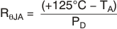
On both the VSON (DRC) and VQFN (RGW) packages, the primary conduction path for heat is through the exposed pad to the printed circuit board (PCB). The pad can be connected to ground or be left floating; however, the pad be attached to an appropriate amount of copper PCB area to ensure the device does not overheat. The maximum junction-to-ambient thermal resistance depends on the maximum ambient temperature, maximum device junction temperature, and power dissipation of the device and can be calculated using Equation 7:
Knowing the maximum RθJA, the minimum amount of PCB copper area needed for appropriate heat sinking can be estimated using Figure 8-13.

Figure 8-13 shows the variation of RθJA as a function of ground plane copper area in the board. This figure is intended only as a guideline to demonstrate the effects of heat spreading in the ground plane and is not intended to be used to estimate actual thermal performance in real application environments.