SBVS083E January 2007 – January 2015 TPS780
PRODUCTION DATA.
- 1 Features
- 2 Applications
- 3 Description
- 4 Revision History
- 5 Pin Configuration and Functions
- 6 Specifications
- 7 Detailed Description
- 8 Application and Implementation
- 9 Power Supply Recommendations
- 10Layout
- 11Device and Documentation Support
- 12Mechanical, Packaging, and Orderable Information
Package Options
Mechanical Data (Package|Pins)
Thermal pad, mechanical data (Package|Pins)
- DRV|6
Orderable Information
6 Specifications
6.1 Absolute Maximum Ratings
over operating free-air temperature range (unless otherwise noted) (1)| MIN | MAX | UNIT | ||
|---|---|---|---|---|
| Voltage | VIN | –0.3 | +6.0 | V |
| VEN and VVSET | –0.3 | VIN + 0.3(2) | ||
| VOUT | –0.3 | VIN + 0.3 | ||
| Current | IOUT | Internally limited | ||
| Output short-circuit duration | Indefinite | |||
| Total continuous power dissipation, PDISS | See Thermal Information | |||
| Temperature | Operating junction, TJ | –40 | 125 | °C |
| Storage, Tstg | –55 | 150 | °C | |
(1) Stresses beyond those listed under Absolute Maximum Ratings may cause permanent damage to the device. These are stress ratings only, which do not imply functional operation of the device at these or any other conditions beyond those indicated under Recommended Operating Conditions. Exposure to absolute-maximum-rated conditions for extended periods may affect device reliability.
(2) VEN and VVSET absolute maximum rating are VIN + 0.3V or +6.0V, whichever is less.
6.2 ESD Ratings
| VALUE | UNIT | |||
|---|---|---|---|---|
| V(ESD) | Electrostatic discharge | Human body model (HBM), per ANSI/ESDA/JEDEC JS-001, all pins(1) | ±2000 | V |
| Charged device model (CDM), per JEDEC specification JESD22-C101, all pins(2) | ±500 | |||
(1) JEDEC document JEP155 states that 500-V HBM allows safe manufacturing with a standard ESD control process.
(2) JEDEC document JEP157 states that 250-V CDM allows safe manufacturing with a standard ESD control process.
6.3 Recommended Operating Conditions
over operating junction temperature range (unless otherwise noted)| MIN | NOM | MAX | UNIT | ||
|---|---|---|---|---|---|
| VIN | Input voltage | 2.2 | 5.5 | V | |
| VOUT | Output voltage | 1.8 | 4.2 | V | |
| VEN | Enable voltage | 0 | VIN | V | |
| IOUT | Output current | 0 | 150 | mA | |
| TJ | Junction temperature | –40 | 125 | °C | |
6.4 Thermal Information
| THERMAL METRIC(1) | TPS780xx | UNIT | ||
|---|---|---|---|---|
| DDC | DRV | |||
| 5 PINS | 6 PINS | |||
| RθJA | Junction-to-ambient thermal resistance | 193.0 | 65.9 | °C/W |
| RθJC(top) | Junction-to-case (top) thermal resistance | 40.1 | 87.3 | |
| RθJB | Junction-to-board thermal resistance | 34.3 | 35.4 | |
| ψJT | Junction-to-top characterization parameter | 0.9 | 1.7 | |
| ψJB | Junction-to-board characterization parameter | 34.1 | 35.8 | |
| RθJC(bot) | Junction-to-case (bottom) thermal resistance | N/A | 6.1 | |
(1) For more information about traditional and new thermal metrics, see the IC Package Thermal Metrics application report, SPRA953.
6.5 Electrical Characteristics
Over operating temperature range (TJ = –40°C to 125°C), VIN = VOUT(nom) + 0.5 V or 2.2 V, whichever is greater; IOUT = 100 μA, VVSET = VEN = VIN, COUT = 1.0 μF, fixed or adjustable, unless otherwise noted. Typical values at TJ = 25°C.| PARAMETER | TEST CONDITIONS | MIN | TYP | MAX | UNIT | |||
|---|---|---|---|---|---|---|---|---|
| VIN | Input voltage range | 2.2 | 5.5 | V | ||||
| VOUT(1) | DC output accuracy | Nominal | TJ = 25°C, VSET = high/low | –2% | ±1% | +2% | ||
| Over VIN, IOUT, temperature | VOUT(nom) + 0.5 V ≤ VIN ≤ 5.5 V, 0 mA ≤ IOUT ≤ 150 mA, VSET = high/low |
–3.0% | ±2.0% | +3.0% | ||||
| VFB | Internal reference(9)
(adjustable version only) |
TJ = 25°C, VIN = 4.0 V, IOUT = 75 mA | 1.216 | V | ||||
| VOUT_RANGE | Output voltage range(2)(3)
(adjustable version only) |
VIN = 5.5 V, IOUT = 100 μA(9) | VFB | 5.25 | V | |||
| ΔVOUT(ΔVIN) | Line regulation | VOUT(nom) + 0.5 V ≤ VIN ≤ 5.5 V, IOUT = 5 mA |
–1% | +1% | ||||
| ΔVOUT(ΔIOUT) | Load regulation | 0 mA ≤ IOUT ≤ 150 mA | –2% | +2% | ||||
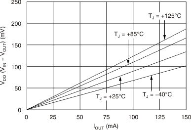
| VDO | Dropout voltage(4) | VIN = 95% VOUT(nom), IOUT = 150 mA | 250 | mV | ||||
| Vn | Output noise voltage | BW = 100 Hz to 100 kHz, VIN = 2.2 V, VOUT = 1.2 V, IOUT = 1 mA |
86 | μVRMS | ||||
| VHI | VSET high (output VOUT(LO) selected), or EN high (enabled) | 1.2 | VIN | V | ||||
| VLO | VSET low (output VOUT(HI) selected), or EN low (disabled) | 0 | 0.4 | V | ||||
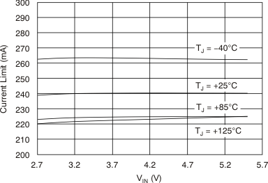
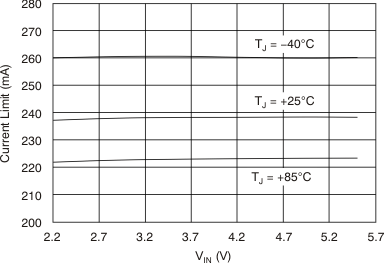
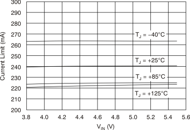
| ICL | Output current limit | VOUT = 0.90 × VOUT(nom) | 150 | 230 | 400 | mA | ||
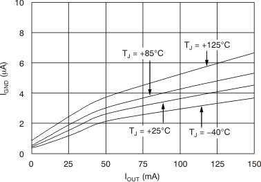
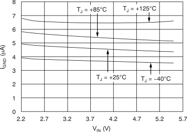
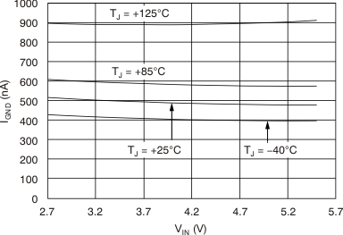
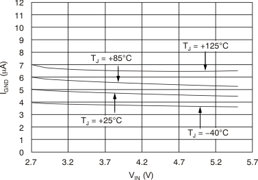
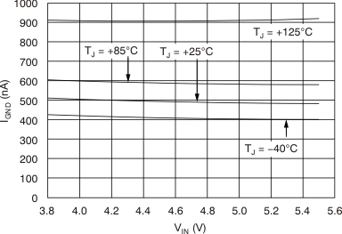
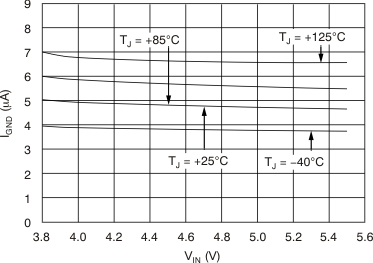
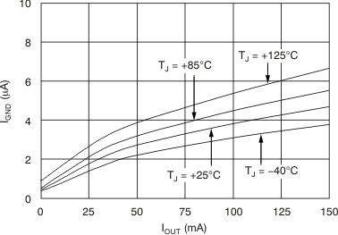
| IGND | Ground pin current | IOUT = 0 mA(5) | 420 | 800 | nA | |||
| IOUT = 150 mA | 5 | μA | ||||||
| ISHDN | Shutdown current (IGND) | VEN ≤ 0.4 V, 2.2 V ≤ VIN < 5.5 V, TJ = –40°C to 100°C |
18 | 130 | nA | |||
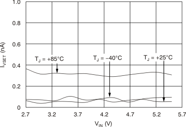
| IVSET | VSET pin current | VEN = VVSET = 5.5 V | 70 | nA | ||||
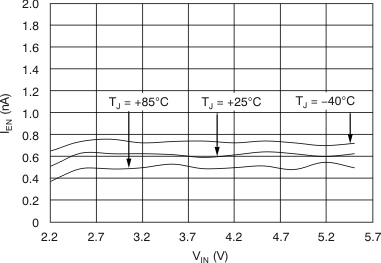
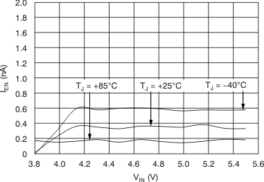
| IEN | EN pin current | VEN = VVSET = 5.5 V | 40 | nA | ||||
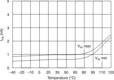
| IFB | FB pin current(10)
(Adjustable version only) |
VIN = 5.5 V, VOUT = 1.2 V, IOUT = 100 μA | 10 | nA | ||||
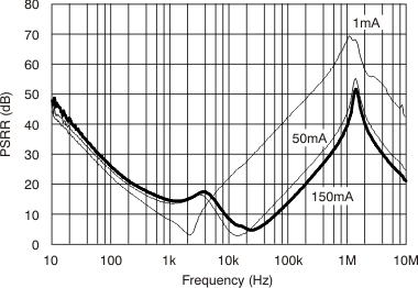
| PSRR | Power-supply rejection ratio | VIN = 4.3 V, VOUT = 3.3 V, IOUT = 150 mA |
f = 10 Hz | 40 | dB | |||
| f = 100 Hz | 20 | |||||||
| f = 1kHz | 15 | |||||||
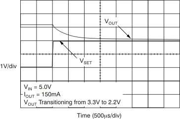
| tTR(H→L) | VOUT transition time (high-to-low) VOUT = 97% × VOUT(HI) |
VOUT_LOW = 2.2 V, VOUT(HI) = 3.3 V, IOUT = 10 mA |
800 | μs | ||||
| tTR(L→H) | VOUT transition time (low-to-high) VOUT = 97% × VOUT(LO) |
VOUT_HIGH = 3.3 V, VOUT(LO) = 2.2 V, IOUT = 10 mA |
800 | μs | ||||
| tSTR | Start-up time(6) | COUT = 1.0 μF, VOUT = 10% VOUT(nom) to VOUT = 90% VOUT(nom) | 500 | μs | ||||
| tSHDN | Shutdown time(7) | IOUT = 150 mA, COUT = 1.0 μF, VOUT = 2.8 V, VOUT = 90% VOUT(nom) to VOUT = 10% VOUT(nom) |
500(8) | μs | ||||
| TSD | Thermal shutdown temperature | Shutdown, temperature increasing | 160 | °C | ||||
| Reset, temperature decreasing | 140 | °C | ||||||
| TJ | Operating junction temperature | –40 | 125 | °C | ||||
(1) The output voltage for VSET = low/high is programmed at the factory.
(2) No VSET pin on the adjustable version.
(3) No dynamic voltage scaling on the adjustable version.
(4) VDO is not measured for devices with VOUT(nom) < 2.3 V because minimum VIN = 2.2 V.
(5) IGND = 800 nA (max) up to 100°C.
(6) Time from VEN = 1.2 V to VOUT = 90% (VOUT(nom)).
(7) Time from VEN = 0.4 V to VOUT = 10% (VOUT(nom)).
(8) See Shutdown for more details.
(9) Adjustable version only.
(10) The TPS78001 FB pin is tied to VOUT. Adjustable version only.
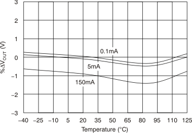
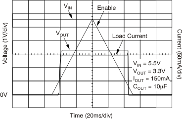
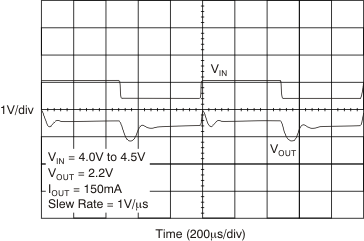
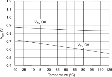
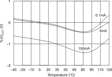
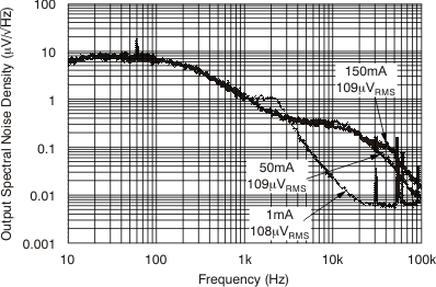
6.6 Typical Characteristics
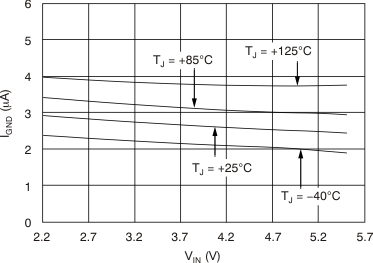
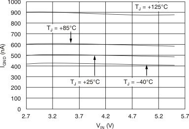
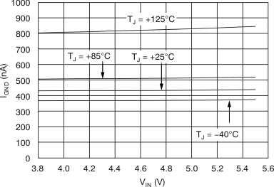
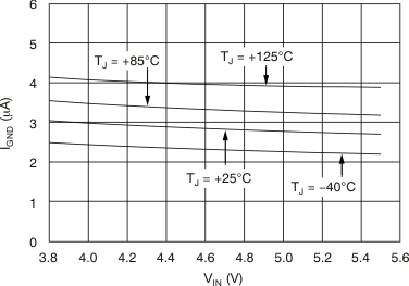
Over the operating temperature range of TJ = –40°C to 125°C, VIN = VOUT(nom) + 0.5 V or 2.2 V, whichever is greater; IOUT = 100 μA, VEN = VVSET = VIN, COUT = 1 μF, and CIN = 1 μF, unless otherwise noted.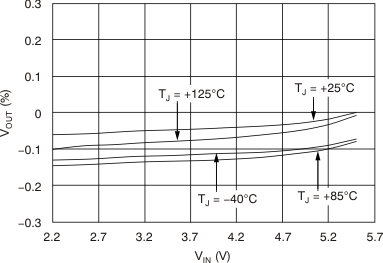
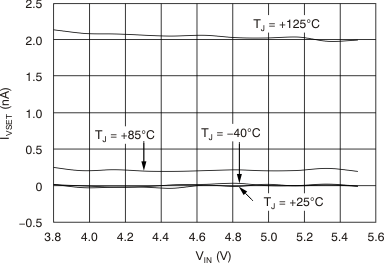
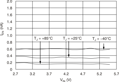
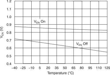
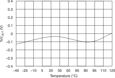
| IOUT = 5 mA | VOUT(nom) = 1.22 V |
| IOUT = 150 mA | VVSET = 1.2 V | VOUT(nom) = 2.2 V |
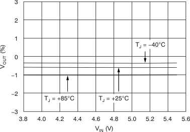
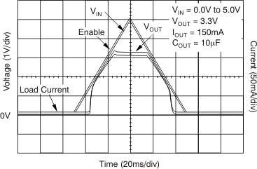
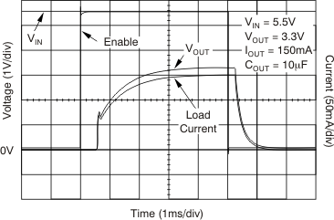
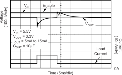
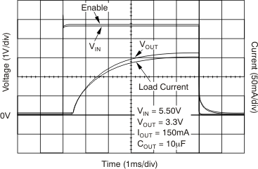
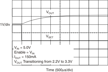
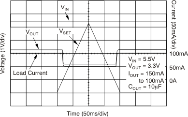
| IOUT = 150 mA | VVSET = 0.4 V | VOUT(nom) = 3.3 V |
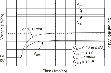
| VVSET = 1.2 V | VIN = 2.7 V | VOUT(nom) = 2.2 V |
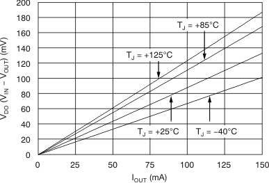
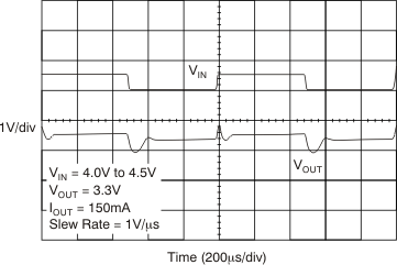
| VOUT(nom) = 3.3 V | VIN = 0.95 × VOUT(nom) | |
| VOUT(nom) = 3.3 | VIN = 0.95 × VOUT(nom) | |
| IOUT = 50 mA | VOUT(nom) = 1.22 V |
| IOUT = 0 mA | VVSET = 1.2 V | VOUT(nom) = 2.2 V |

| IOUT = 50 mA | VVSET = 1.2 V | VOUT(nom) = 2.2 V |
| IOUT = 0 mA | VVSET = 0.4 V | VOUT(nom) = 3.3 V |
| IOUT = 50 mA | VVSET = 0.4 V | VOUT(nom) = 3.3 V |
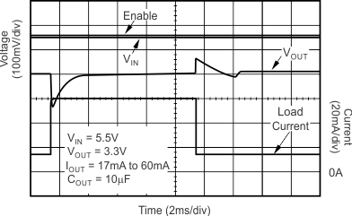
| VVSET = 1.2 V | VIN = 5.5 V | VOUT(nom) = 2.2 V |
| IOUT = 0 mA | VVSET = 0.4 V |
| VVSET = 1.2 V | VOUT = 95% VOUT(nom) | VOUT(nom) = 2.2 V |
| IOUT = 0 mA | VOUT(nom) = 1.22 V |
| IOUT = 100 μA | VVSET = 0.4 V | VOUT(nom) = 3.3 V |
| IOUT = 100 μA | VVSET = 1.2 V | VOUT(nom) = 2.2 V |
| IOUT = 1 mA |
| IOUT = 1 mA | VIN = 3.8 V | VOUT(nom) = 3.3 V |
| VVSET = 0.4 V | VIN = 3.8 V | VOUT(nom) = 3.3 V |
| VIN = 2.7 V | VOUT = 1.2 V | COUT = 2.2 μF |
| IOUT = 5 mA | VVSET = 1.2 V | VOUT(nom) = 2.2 V | |
| IOUT = 5 mA | VVSET = 0.4 V | VOUT(nom) = 3.3 V |
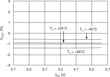
| VOUT(nom) = 3.3 V |
| VVSET = 0.4 V | VIN = 3.8 V | VOUT(nom) = 3.3 V |
| VVSET = 0.4 V | VOUT(nom) = 3.3 V | VIN = 0.95 × VOUT(nom) |

| VVSET = 0.4 V | VOUT(nom) = 3.3 V | VIN = 0.95 × VOUT(nom) |
| IOUT = 150 mA | VOUT(nom) = 1.22 V |
| IOUT = 1 mA | VVSET = 1.2 V | VOUT(nom) = 2.2 V |
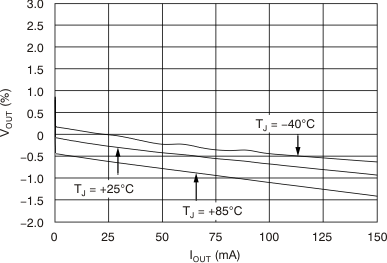
| IOUT = 150 mA | VVSET = 1.2 V | VOUT(nom) = 2.2 V |
| IOUT = 1 mA | VVSET = 0.4 V | VOUT(nom) = 3.3 V |
| IOUT = 150 mA | VVSET = 0.4 V | VOUT(nom) = 3.3 V |
| VVSET = 0.4 V | VIN = 5.5 V | VOUT(nom) = 3.3 V |
| VOUT = 90% VOUT(nom) | VOUT(nom) = 1.22 V | |
| VVSET = 0.4 V | VOUT = 95% VOUT(nom) | VOUT(nom) = 3.3 V |
| IOUT = 100 μA | VVSET = 1.2 V | VOUT(nom) = 2.2 V |
| IOUT = 1 mA | VOUT(nom) = 1.22 V |
| IOUT = 100 μA | VVSET = 0.4 V | VOUT(nom) = 3.3 V |
| IOUT = 1 mA |
| VVSET = 1.2 V | VIN = 2.7 V | VOUT(nom) = 2.2 V |
| CIN = 1 μF | COUT = 2.2 μF | VVSET = 1.2 V |
| VIN = 2.7 V |