SBVS398A December   2021  – September 2022 TPS7A21

PRODUCTION DATA  

  1. Features
  2. Applications
  3. Description
  4. Revision History
  5. Pin Configuration and Functions
  6. Specifications
    1. 6.1 Absolute Maximum Ratings
    2. 6.2 ESD Ratings
    3. 6.3 Recommended Operating Conditions
    4. 6.4 Thermal Information
    5. 6.5 Electrical Characteristics
    6. 6.6 Typical Characteristics
  7. Detailed Description
    1. 7.1 Overview
    2. 7.2 Functional Block Diagram
    3. 7.3 Feature Description
      1. 7.3.1 Smart Enable (EN)
      2. 7.3.2 Low Output Noise
      3. 7.3.3 Active Discharge
      4. 7.3.4 Dropout Voltage
      5. 7.3.5 Foldback Current Limit
      6. 7.3.6 Undervoltage Lockout
      7. 7.3.7 Thermal Overload Protection (TSD)
    4. 7.4 Device Functional Modes
      1. 7.4.1 Device Functional Mode Comparison
      2. 7.4.2 Normal Operation
      3. 7.4.3 Dropout Operation
      4. 7.4.4 Disabled
  8. Applications and Implementation
    1. 8.1 Application Information
      1. 8.1.1 Recommended Capacitor Types
      2. 8.1.2 Input and Output Capacitor Requirements
      3. 8.1.3 Load Transient Response
      4. 8.1.4 Undervoltage Lockout (UVLO) Operation
      5. 8.1.5 Power Dissipation (PD)
      6. 8.1.6 Estimating Junction Temperature
      7. 8.1.7 Recommended Area For Continuous Operation
    2. 8.2 Typical Application
      1. 8.2.1 Design Requirements
      2. 8.2.2 Detailed Design Procedure
        1. 8.2.2.1 Power Dissipation and Device Operation
      3. 8.2.3 Application Curves
    3. 8.3 Power Supply Recommendations
    4. 8.4 Layout
      1. 8.4.1 Layout Guidelines
        1. 8.4.1.1 DSBGA Mounting
        2. 8.4.1.2 DSBGA Light Sensitivity
      2. 8.4.2 Layout Example
  9. Device and Documentation Support
    1. 9.1 Device Support
      1. 9.1.1 Device Nomenclature
    2. 9.2 Documentation Support
      1. 9.2.1 Related Documentation
    3. 9.3 Receiving Notification of Documentation Updates
    4. 9.4 Support Resources
    5. 9.5 Trademarks
    6. 9.6 Electrostatic Discharge Caution
    7. 9.7 Glossary
  10. 10Mechanical, Packaging, and Orderable Information
    1. 10.1 Mechanical Data

Package Options

Refer to the PDF data sheet for device specific package drawings

Mechanical Data (Package|Pins)
  • YWD|4
Thermal pad, mechanical data (Package|Pins)
Orderable Information

Description

The TPS7A21 is an ultra-small, low-dropout (LDO) linear voltage regulator that can source 500 mA of output current. The device provides low noise, high PSRR, and excellent load and line transient performance to meet the requirements of RF and other sensitive analog circuits. Innovative design techniques result in low-noise performance without the addition of an external noise bypass capacitor. With the device low quiescent current, the TPS7A21 is a good choice for battery-powered systems. The 2.0-V to 6.0-V input voltage range and 0.8-V to 5.5-V output voltage range support a variety of system requirements. The internal precision reference circuit enables excellent accuracy; the maximum output voltage tolerance is 1.5% over load, line, and temperature variations.

An internal soft-start circuit helps control the inrush current, thus minimizing the input voltage drop during start up. The LDO is stable with small ceramic capacitors, allowing for a small overall solution size.

A smart enable input circuit with an internally controlled pulldown resistor keeps the LDO disabled even when the EN pin is unconnected and helps eliminate external components that are otherwise required to pull down the EN input.

Package Information(1)
PART NUMBERPACKAGEBODY SIZE (NOM)
TPS7A21YWD (DSBGA, 4)0.602 mm × 0.602 mm
For all available packages, see the orderable addendum at the end of the data sheet.
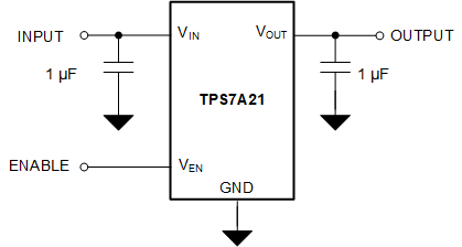
GUID-20211119-SS0I-MLRB-WXLG-KZ03CDPGJ8KG-low.gif Simplified Schematic