SLVSAA0E November   2010  – March 2020 TPS7A6201-Q1

PRODUCTION DATA.  

  1. Features
  2. Applications
  3. Description
    1.     Device Images
      1.      Typical Regulator Stability
      2.      Application Schematic
  4. Revision History
  5. Pin Configuration and Functions
    1.     Pin Functions
  6. Specifications
    1. 6.1 Absolute Maximum Ratings
    2. 6.2 ESD Ratings
    3. 6.3 Recommended Operating Conditions
    4. 6.4 Thermal Information
    5. 6.5 Electrical Characteristics
    6. 6.6 Typical Characteristics
  7. Detailed Description
    1. 7.1 Overview
    2. 7.2 Functional Block Diagram
    3. 7.3 Feature Description
      1. 7.3.1 Power Up
      2. 7.3.2 Adjustable Output Voltage
      3. 7.3.3 Enable Input
      4. 7.3.4 Charge Pump Operation
      5. 7.3.5 Undervoltage Shutdown
      6. 7.3.6 Low Voltage Tracking
      7. 7.3.7 Integrated Fault Protection
      8. 7.3.8 Thermal Shutdown
    4. 7.4 Device Functional Modes
      1. 7.4.1 Low Power Mode
  8. Application and Implementation
    1. 8.1 Application Information
    2. 8.2 Typical Application
      1. 8.2.1 Design Requirements
      2. 8.2.2 Detailed Design Procedure
        1. 8.2.2.1 Input Capacitor
        2. 8.2.2.2 Output Capacitor
        3. 8.2.2.3 Feedback Resistor
      3. 8.2.3 Application Curve
  9. Power Supply Recommendations
  10. 10Layout
    1. 10.1 Layout Guidelines
      1. 10.1.1 Power Dissipation and Thermal Considerations
    2. 10.2 Layout Example
  11. 11Device and Documentation Support
    1. 11.1 Receiving Notification of Documentation Updates
    2. 11.2 Community Resources
    3. 11.3 Trademarks
    4. 11.4 Electrostatic Discharge Caution
    5. 11.5 Glossary
  12. 12Mechanical, Packaging, and Orderable Information

Package Options

Refer to the PDF data sheet for device specific package drawings

Mechanical Data (Package|Pins)
  • KTT|5
Thermal pad, mechanical data (Package|Pins)
Orderable Information

Charge Pump Operation

This device has an internal charge pump which turns on or off depending on the input voltage and the output current. The charge pump switching circuitry shall not cause conducted emissions to exceed required thresholds on the input voltage line. For a given output current, the charge pump stays on at lower input voltages and turns off at higher input voltages. The charge pump switching thresholds are hysteretic. Figure 16 and Figure 17 shows typical switching thresholds for the charge pump at light (IOUT < ~2 mA) and heavy (IOUT > ~2 mA) loads respectively.
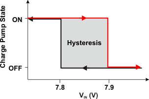
TPS7A6201-Q1 charge_pump_light_load_lvsa62.gifFigure 16. Charge Pump Operation at Light Loads
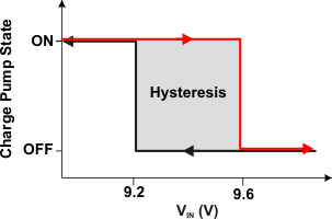
TPS7A6201-Q1 charge_pump_heavy_load_lvsa62.gifFigure 17. Charge Pump Operation at Heavy Loads