SLVSAA0E November 2010 – March 2020 TPS7A6201-Q1
PRODUCTION DATA.
- 1 Features
- 2 Applications
- 3 Description
- 4 Revision History
- 5 Pin Configuration and Functions
- 6 Specifications
- 7 Detailed Description
- 8 Application and Implementation
- 9 Power Supply Recommendations
- 10Layout
- 11Device and Documentation Support
- 12Mechanical, Packaging, and Orderable Information
Package Options
Refer to the PDF data sheet for device specific package drawings
Mechanical Data (Package|Pins)
- KTT|5
Thermal pad, mechanical data (Package|Pins)
- KTT|5
Orderable Information
10.1.1 Power Dissipation and Thermal Considerations
Calculate the power dissipated in the device using Equation 3.
where
- PD = continuous power dissipation
- IOUT = output current
- VIN = input voltage
- VOUT = output voltage
- IQUIESCENT = quiescent current
As IQUIESCENT << IOUT, therefore, the term IQUIESCENT × VIN in Equation 3 can be ignored.
For device under operation at a given ambient air temperature (TA), calculate the junction temperature (TJ) Equation 4.
where
- RθJA = junction to ambient air thermal impedance
Calculate the rise in junction temperature due to power dissipation using Equation 5.
For a given maximum junction temperature (TJ-Max), calculate the maximum ambient air temperature (TA-Max) at which the device can operate using Equation 6.
Example
If IOUT = 100 mA, VOUT = 5 V, VIN = 14 V, IQUIESCENT = 250 µA, and RθJA = 30˚C/W, the continuous power dissipated in the device is 0.9 W. The rise in junction temperature due to power dissipation is 27˚C. For a maximum junction temperature of 150˚C, maximum ambient air temperature at which the device can operate is 123˚C.
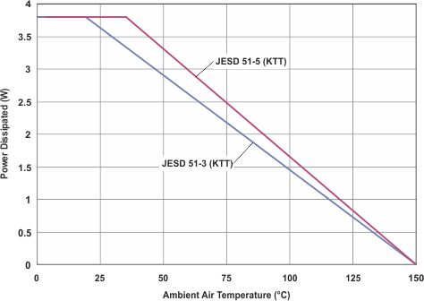
For adequate heat dissipation, TI recommends soldering the thermal pad (exposed heat sink) to thermal land pad on the PCB. Doing this provides a heat conduction path from die to the PCB and reduces overall package thermal resistance. Figure 22 illustrates the power derating curves for the TPS7A6201-Q1 device in the KTT (TO-263) package..
 Figure 22. Power Derating Curves
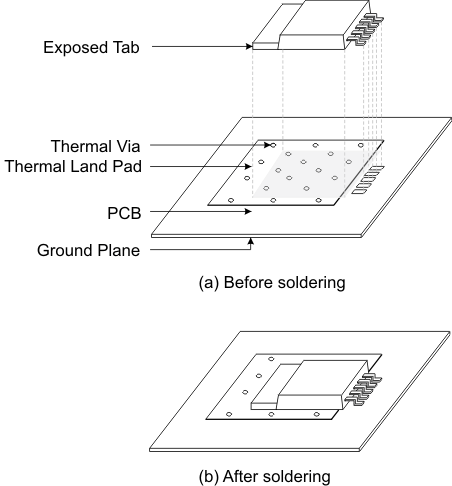
 For optimum thermal performance, TI recommends using a high-K PCB with thermal vias between ground plane and solder pad or thermal land pad. This is shown in Figure 23 (a) and (b). Furthermore, heat spreading capabilities of a PCB can be considerably improved by using a thicker ground plane and a thermal land pad with a larger surface area.
 Figure 23. Using Multilayer PCB and Thermal Vias for Adequate Heat Dissipation
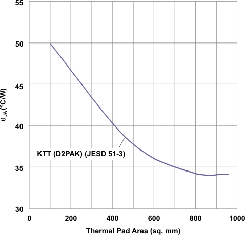
 Keeping other factors constant, surface area of the thermal land pad contributes to heat dissipation only to a certain extent. Figure 24 shows a variation of RθJA with surface area of the thermal land pad (soldered to the exposed pad) for KTT package.
 Figure 24. RθJA vs Thermal Pad Area