SBVS416B May   2022  – August 2022 TPS7A74

PRODUCTION DATA  

  1. Features
  2. Applications
  3. Description
  4. Revision History
  5. Pin Configuration and Functions
  6. Specifications
    1. 6.1 Absolute Maximum Ratings
    2. 6.2 ESD Ratings
    3. 6.3 Recommended Operating Conditions
    4. 6.4 Thermal Information
    5. 6.5 Electrical Characteristics
    6. 6.6 Typical Characteristics
  7. Detailed Description
    1. 7.1 Overview
    2. 7.2 Functional Block Diagram
    3. 7.3 Feature Description
      1. 7.3.1 Enable and Shutdown
      2. 7.3.2 Active Discharge
      3. 7.3.3 Global Undervoltage Lockout (UVLO) Circuit
      4. 7.3.4 Internal Current Limit
      5. 7.3.5 Thermal Shutdown Protection (TSD)
    4. 7.4 Device Functional Modes
      1. 7.4.1 Normal Operation
      2. 7.4.2 Dropout Operation
      3. 7.4.3 Disabled
    5. 7.5 Programming
      1. 7.5.1 Programmable Soft-Start
      2. 7.5.2 Sequencing Requirements
  8. Application and Implementation
    1. 8.1 Application Information
      1. 8.1.1 Adjusting the Output Voltage
      2. 8.1.2 Input, Output, and Bias Capacitor Requirements
      3. 8.1.3 Transient Response
      4. 8.1.4 Dropout Voltage
      5. 8.1.5 Output Noise
      6. 8.1.6 Estimating Junction Temperature
    2. 8.2 Typical Application
      1. 8.2.1 FPGA I/O Supply at 1.8 V With a Bias Rail
        1. 8.2.1.1 Design Requirements
        2. 8.2.1.2 Detailed Design Procedure
        3. 8.2.1.3 Application Curves
    3. 8.3 Power Supply Recommendations
    4. 8.4 Layout
      1. 8.4.1 Layout Guidelines
        1. 8.4.1.1 Estimating Junction Temperature
      2. 8.4.2 Layout Example
  9. Device and Documentation Support
    1. 9.1 Device Support
      1. 9.1.1 Development Support
        1. 9.1.1.1 Evaluation Modules
        2. 9.1.1.2 Spice Models
    2. 9.2 Documentation Support
      1. 9.2.1 Related Documentation
    3. 9.3 Receiving Notification of Documentation Updates
    4. 9.4 Support Resources
    5. 9.5 Trademarks
    6. 9.6 Electrostatic Discharge Caution
    7. 9.7 Glossary
  10. 10Mechanical, Packaging, and Orderable Information

Package Options

Mechanical Data (Package|Pins)
Thermal pad, mechanical data (Package|Pins)
Orderable Information

Global Undervoltage Lockout (UVLO) Circuit

Two undervoltage lockout (UVLO) circuits are present to prevent the TPS7A74 from turning on with an insufficient rail. One circuit is present on the BIAS pin and the other circuit is on the IN pin. The two UVLO signals are connected internally through an AND gate, as shown in Figure 7-1, that turns off the device when the voltage on either input is below their respective UVLO thresholds.

In other words, the output is disabled until the IN pin voltage reaches a value greater than UVLOIN and the BIAS pin voltage reaches a voltage greater than UVLOBIAS.
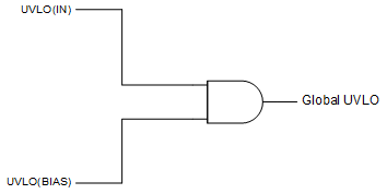
GUID-20220314-SS0I-DZ96-FHHN-KLC1VQZDTFFN-low.gif Figure 7-1 Global UVLO Circuit