SBVS343A March 2019 – September 2019 TPS7A78
PRODUCTION DATA.
- 1 Features
- 2 Applications
- 3 Description
- 4 Revision History
- 5 Pin Configuration and Functions
- 6 Specifications
-
7 Detailed Description
- 7.1 Overview
- 7.2 Functional Block Diagram
- 7.3
Feature Description
- 7.3.1 Active Bridge Control
- 7.3.2 Full-Bridge (FB) and Half-Bridge (HB) Configurations
- 7.3.3 4:1 Switched-Capacitor Voltage Reduction
- 7.3.4 Undervoltage Lockout Circuits (VUVLO_SCIN) and (VUVLO_LDO_IN)
- 7.3.5 Dropout Voltage Regulation
- 7.3.6 Current Limit
- 7.3.7 Programmable Power-Fail Detection
- 7.3.8 Power-Good (PG) Detection
- 7.3.9 Thermal Shutdown
- 7.4 Device Functional Modes
-
8 Application and Implementation
- 8.1
Application Information
- 8.1.1 Recommended Capacitor Types
- 8.1.2 Input and Output Capacitors Requirements
- 8.1.3 Startup Behavior
- 8.1.4 Load Transient
- 8.1.5 Standby Power and Output Efficiency
- 8.1.6 Reverse Current
- 8.1.7 Switched-Capacitor Stage Output Impedance
- 8.1.8 Power Dissipation (PD)
- 8.1.9 Estimating Junction Temperature
- 8.2
Typical Application
- 8.2.1 Design Requirements
- 8.2.2
Detailed Design Procedure
- 8.2.2.1 Calculating the Cap-Drop Capacitor CS
- 8.2.2.2 Calculating the Surge Resistor RS
- 8.2.2.3 Checking for the Device Maximum ISHUNT Current
- 8.2.2.4 Calculating the Bulk Capacitor CSCIN
- 8.2.2.5 Calculating the PFD Pin Resistor Dividers for a Power-Fail Detection
- 8.2.2.6 Summary of the Typical Application Design Components
- 8.2.3 Application Curves
- 8.1
Application Information
- 9 Power Supply Recommendations
- 10Layout
- 11Device and Documentation Support
- 12Mechanical, Packaging, and Orderable Information
Package Options
Mechanical Data (Package|Pins)
- PWP|14
Thermal pad, mechanical data (Package|Pins)
- PWP|14
Orderable Information
8.1.3 Startup Behavior
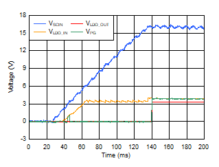
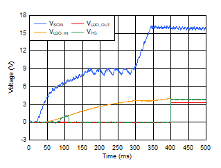
The device startup time is dependent on the circuit topology (FB versus HB configuration), AC supply voltage and frequency, input capacitors values, and output voltage. The FB configuration has a faster startup time compared to the HB configuration. Having a larger than minimum CS capacitor value shortens the startup time without exceeding the maximum ISHUNT current specified in the Recommended Operating Conditions table. However, startup behavior depends on which CSCIN and CLDO_IN capacitor values are used. Figure 19 illustrates the startup behavior with the minimum required CSCIN capacitor and a typical CLDO_IN capacitor to support 30 mA of load current with the FB configuration. Figure 20 illustrates the startup behavior with the minimum required CSCIN capacitor and a large CLDO_IN capacitor in the same configuration.
Although the load current has no effect on startup time or startup behavior, the bulk capacitor CSCIN and input capacitor CLDO_IN have a significant effect on the time and behavior; see Figure 19 and Figure 20. For some applications, larger CSCIN or CLDO_IN capacitors are used to hold-up the output voltage on for a longer period of time after the input collapses.

| VAC = 120 VRMS at 60 Hz, FB, CS = 220 nF,
VLDO_OUT = 3.3 V, CSCIN = 47 µF, CLDO_IN = 1 µF, IOUT = 30 mA |
||

| VAC = 120 VRMS at 60 Hz, FB, CS = 220 nF,
VLDO_OUT = 3.3 V, CSCIN = 47 µF, CLDO_IN = 330 µF, IOUT = 30 mA |