SBVS415A april 2023 – july 2023 TPS7A96
PRODUCTION DATA
- 1
- 1 Features
- 2 Applications
- 3 Description
- 4 Revision History
- 5 Pin Configuration and Functions
- 6 Specifications
-
7 Detailed Description
- 7.1 Overview
- 7.2 Functional Block Diagram
- 7.3
Feature Description
- 7.3.1 Output Voltage Setting and Regulation
- 7.3.2 Ultra-Low Noise and Ultra-High Power-Supply Rejection Ratio (PSRR)
- 7.3.3 Programmable Current Limit and Power-Good Threshold
- 7.3.4 Programmable Soft-Start (NR/SS Pin)
- 7.3.5 Precision Enable and UVLOs
- 7.3.6 Active Discharge
- 7.3.7 Thermal Shutdown Protection (TSD)
- 7.4 Device Functional Modes
-
8 Application and Implementation
- 8.1
Application Information
- 8.1.1 Output Voltage Restart (Overshoot Prevention Circuit)
- 8.1.2 Precision Enable (External UVLO)
- 8.1.3 Undervoltage Lockout (UVLO) Operation
- 8.1.4 Dropout Voltage (VDO)
- 8.1.5 Power-Good Feedback (FB_PG Pin) and Power-Good Threshold (PG Pin)
- 8.1.6 Adjusting the Factory-Programmed Current Limit
- 8.1.7 Programmable Soft-Start and Noise-Reduction (NR/SS Pin)
- 8.1.8 Inrush Current
- 8.1.9 Optimizing Noise and PSRR
- 8.1.10 Adjustable Operation
- 8.1.11 Paralleling for Higher Output Current and Lower Noise
- 8.1.12 Recommended Capacitor Types
- 8.1.13 Load Transient Response
- 8.1.14 Power Dissipation (PD)
- 8.1.15 Estimating Junction Temperature
- 8.1.16 TPS7A96EVM-106 Thermal Analysis
- 8.2 Typical Application
- 8.3 Power Supply Recommendations
- 8.4 Layout
- 8.1
Application Information
- 9 Device and Documentation Support
- 10Mechanical, Packaging, and Orderable Information
Package Options
Mechanical Data (Package|Pins)
- DSC|10
Thermal pad, mechanical data (Package|Pins)
- DSC|10
Orderable Information
8.1.8 Inrush Current
Inrush current is defined as the current into the LDO at the IN pin during start-up. Inrush current then consists primarily of the sum of load current and the current used to charge the output capacitor. This current is difficult to measure because the input capacitor must be removed. Operating without an input capacitor is not recommended because this capacitor is required for stability. However, Equation 6 can be used to estimate this current.
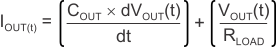
where:
- VOUT(t) is the instantaneous output voltage of the turn-on ramp
- dVOUT(t) / dt is the slope of the VOUT ramp
- RLOAD is the resistive load impedance
As illustrated in Figure 8-10, the external capacitor at the NR/SS pin (CNR/SS) sets the output start-up time by setting the rise time of the VNR/SS reference voltage.
Inrush current for a no-load condition is given in Figure 6-28 to Figure 6-31.