SBVS360A February   2020  – November 2020 TPS7B85-Q1

PRODUCTION DATA  

  1. Features
  2. Applications
  3. Description
  4. Revision History
  5. Pin Configuration and Functions
  6. Specifications
    1. 6.1 Absolute Maximum Ratings
    2. 6.2 ESD Ratings
    3. 6.3 Recommended Operating Conditions
    4. 6.4 Thermal Information
    5. 6.5 Electrical Characteristics
    6. 6.6 Switching Characteristics
    7. 6.7 Typical Characteristics
  7. Detailed Description
    1. 7.1 Overview
    2. 7.2 Functional Block Diagram
    3. 7.3 Feature Description
      1. 7.3.1 Enable (EN)
      2. 7.3.2 Power-Good (PG)
        1. 7.3.2.1 Adjustable Power-Good (PGADJ)
      3. 7.3.3 Adjustable Power-Good Delay Timer (DELAY)
      4. 7.3.4 Sense Comparator
      5. 7.3.5 Undervoltage Lockout
      6. 7.3.6 Thermal Shutdown
      7. 7.3.7 Current Limit
    4. 7.4 Device Functional Modes
      1. 7.4.1 Device Functional Mode Comparison
      2. 7.4.2 Normal Operation
      3. 7.4.3 Dropout Operation
      4. 7.4.4 Disabled
  8. Application and Implementation
    1. 8.1 Application Information
      1. 8.1.1 Input and Output Capacitor Selection
      2. 8.1.2 Dropout Voltage
      3. 8.1.3 Reverse Current
      4. 8.1.4 Power Dissipation (PD)
        1. 8.1.4.1 Thermal Performance Versus Copper Area
      5. 8.1.5 Estimating Junction Temperature
      6. 8.1.6 SI Pin
        1. 8.1.6.1 Calculating the Sense Input (SI) Pin Threshold
        2. 8.1.6.2 Different Uses for the Sense Input Pin
          1. 8.1.6.2.1 Monitoring Input Voltage
          2. 8.1.6.2.2 Creating OV and UV Power-Good
          3. 8.1.6.2.3 Monitoring a Separate Supply Voltage
      7. 8.1.7 Pulling Up the SO and PG Pins to a Different Voltage
      8. 8.1.8 Power-Good
        1. 8.1.8.1 Setting the Adjustable Power-Good Threshold
        2. 8.1.8.2 Setting the Adjustable Power-Good Delay
    2. 8.2 Typical Application
      1. 8.2.1 Design Requirements
      2. 8.2.2 Detailed Design Procedure
        1. 8.2.2.1 Input Capacitor
        2. 8.2.2.2 Output Capacitor
      3. 8.2.3 Application Curves
  9. Power Supply Recommendations
  10. 10Layout
    1. 10.1 Layout Guidelines
      1. 10.1.1 Package Mounting
      2. 10.1.2 Board Layout Recommendations to Improve PSRR and Noise Performance
    2. 10.2 Layout Example
  11. 11Device and Documentation Support
    1. 11.1 Device Support
      1. 11.1.1 Device Nomenclature
    2. 11.2 Receiving Notification of Documentation Updates
    3. 11.3 Support Resources
    4. 11.4 Trademarks
    5. 11.5 Electrostatic Discharge Caution
    6. 11.6 Glossary

Package Options

Mechanical Data (Package|Pins)
Thermal pad, mechanical data (Package|Pins)
Orderable Information

Description

The TPS7B85-Q1 is a low-dropout linear regulator designed to connect to the battery in automotive applications. The device has an input voltage range extending to 40 V, which allows the device to withstand transients (such as load dump) that are anticipated in automotive systems. With only an 18-µA quiescent current, the device is an optimal solution for powering always-on components such as microcontrollers (MCUs) and controller area network (CAN) transceivers in standby systems.

The device has state-of-the-art transient response that allows the output to quickly react to changes in load or line (for example, during cold-crank conditions). Additionally, the device has a novel architecture that minimizes output overshoot when recovering from dropout. During normal operation, the device has a tight DC accuracy of ±0.75% over line, load, and temperature.

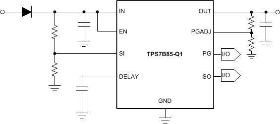
The TPS7B85-Q1 is equipped with power-good and integrated voltage monitoring. The power-good delay and voltage threshold can be adjusted by external components. The integrated voltage detector can be used to monitor the input voltage and alert downstream components (such as MCUs) when the battery voltage begins to fall.

The device is available in a small VSON package that facilitates a compact printed circuit board (PCB) design. The low thermal resistance enables sustained operation despite significant dissipation across the device.

Device Information(1)
PART NUMBER PACKAGE BODY SIZE (NOM)
TPS7B85-Q1 VSON (10) 3.00 mm × 3.00 mm
For all available packages, see the orderable addendum at the end of the data sheet.
GUID-FA99B836-47D9-4BB9-B95A-44DC5F97385F-low.gif Typical Application Schematic