SLVSDW6C April   2017  – April 2021 TPS7H1101A-SP

PRODUCTION DATA  

  1. Features
  2. Applications
  3. Description
  4. Revision History
  5. Pin Configuration and Functions
  6. Specifications
    1. 6.1 Absolute Maximum Ratings
    2. 6.2 ESD Ratings
    3. 6.3 Recommended Operating Conditions
    4. 6.4 Thermal Information
    5. 6.5 Electrical Characteristics
    6. 6.6 Typical Characteristics
  7. Detailed Description
    1. 7.1 Overview
    2. 7.2 Functional Block Diagram
    3. 7.3 Feature Description
      1. 7.3.1 Soft Start
      2. 7.3.2 Power Good (PG)
    4. 7.4 Device Functional Modes
      1. 7.4.1 Enable/Disable
  8. Application and Implementation
    1. 8.1 Application Information
      1. 8.1.1 Stability
    2. 8.2 Typical Application
      1. 8.2.1 Detailed Design Procedure
        1. 8.2.1.1 Adjustable Output Voltage (Feedback Circuit)
        2. 8.2.1.2 PCL
        3. 8.2.1.3 High-Side Current Sense
        4. 8.2.1.4 Current Foldback
        5. 8.2.1.5 Transient Response
        6. 8.2.1.6 Current Sharing
        7. 8.2.1.7 Compensation
        8. 8.2.1.8 Output Noise
        9. 8.2.1.9 Capacitors
      2. 8.2.2 Application Curves
  9. Power Supply Recommendations
  10. 10Layout
    1. 10.1 Layout Guidelines
    2. 10.2 Layout Example
  11. 11Device and Documentation Support
    1. 11.1 Device Support
      1. 11.1.1 Third-Party Products Disclaimer
      2. 11.1.2 Device Nomenclature
    2. 11.2 Documentation Support
      1. 11.2.1 Related Documentation
    3. 11.3 Receiving Notification of Documentation Updates
    4. 11.4 Support Resources
    5. 11.5 Trademarks
    6. 11.6 Electrostatic Discharge Caution
    7. 11.7 Glossary
  12. 12Mechanical, Packaging, and Orderable Information

Package Options

Mechanical Data (Package|Pins)
Thermal pad, mechanical data (Package|Pins)
Orderable Information

Power Good (PG)

Power Good terminal (9) is an open-drain connection and can be used to sequence multiple LDOs. Figure 7-1 shows typical connection. The PG terminal will be pulled low until the output voltage reaches 90% of its maximum level. At that point, the PG pin will be pulled up. Since the PG pin is open drain, it can be pulled up to any voltage as long as it does not exceed the absolute max of 7.5 V listed in Section 6.5.
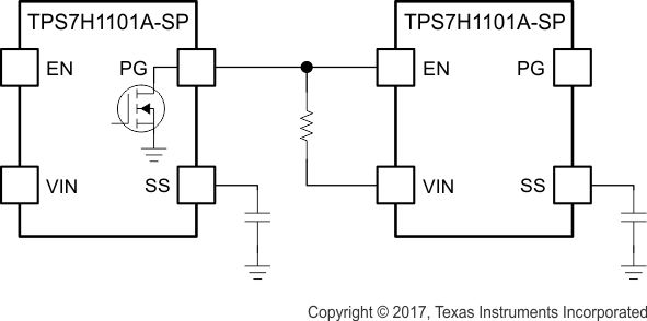
GUID-3698CB0B-C68E-405E-A094-7B085A3F2598-low.gifFigure 7-1 Sequencing LDOs With Power Good
Note:

For PSpice models, WEBENCH, and reference design, see the Design & development tab of the product folder.

  1. PSpice transient model (switching, transient, and stability simulations)
  2. PSpice Worst Case Analysis (WCA) model (radiation and aging stability – Bode plot)