SLVSDN4 June   2017 TPS82150

PRODUCTION DATA.  

  1. Features
  2. Applications
  3. Description
    1.     Device Images
      1.      Typical Application Schematic spacespace
      2.      Efficiency vs Output Current, VIN=12V space
  4. Revision History
  5. Pin Configuration and Functions
    1.     Pin Functions
  6. Specifications
    1. 6.1 Absolute Maximum Ratings
    2. 6.2 ESD Ratings
    3. 6.3 Recommend Operating Conditions
    4. 6.4 Thermal Information
    5. 6.5 Electrical Characteristics
    6. 6.6 Typical Characteristics
  7. Detailed Description
    1. 7.1 Overview
    2. 7.2 Functional Block Diagram
    3. 7.3 Feature Description
      1. 7.3.1 PWM and PSM Operation
      2. 7.3.2 Low Dropout Operation (100% Duty Cycle)
      3. 7.3.3 Switch Current Limit
      4. 7.3.4 Undervoltage Lockout
      5. 7.3.5 Thermal Shutdown
    4. 7.4 Device Functional Modes
      1. 7.4.1 Enable and Disable (EN)
      2. 7.4.2 Soft Startup (SS/TR)
      3. 7.4.3 Voltage Tracking (SS/TR)
      4. 7.4.4 Power Good Output (PG)
  8. Application and Implementation
    1. 8.1 Application Information
    2. 8.2 Typical Applications
      1. 8.2.1 1.8-V Output Application
        1. 8.2.1.1 Design Requirements
        2. 8.2.1.2 Detailed Design Procedure
          1. 8.2.1.2.1 Custom Design with WEBENCH® Tools
          2. 8.2.1.2.2 Setting the Output Voltage
          3. 8.2.1.2.3 Input and Output Capacitor Selection
          4. 8.2.1.2.4 Soft Startup Capacitor Selection
        3. 8.2.1.3 Application Performance Curves
    3. 8.3 System Examples
      1. 8.3.1 Inverting Power Supply
  9. Power Supply Recommendations
  10. 10Layout
    1. 10.1 Layout Guidelines
    2. 10.2 Layout Example
    3. 10.3 Thermal Consideration
  11. 11Device and Documentation Support
    1. 11.1 Device Support
      1. 11.1.1 Third-Party Products Disclaimer
      2. 11.1.2 Development Support
        1. 11.1.2.1 Custom Design With WEBENCH® Tools
    2. 11.2 Receiving Notification of Documentation Updates
    3. 11.3 Community Resources
    4. 11.4 Trademarks
    5. 11.5 Electrostatic Discharge Caution
    6. 11.6 Glossary
  12. 12Mechanical, Packaging, and Orderable Information
    1. 12.1 Package Materials Information
      1. 12.1.1 Tape and Reel Information

Package Options

Mechanical Data (Package|Pins)
  • SIL|8
Thermal pad, mechanical data (Package|Pins)
Orderable Information

Application Performance Curves

TA = 25°C, VIN = 12 V, VOUT = 1.8 V, unless otherwise noted.
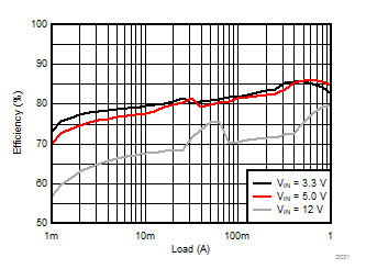
TPS82150 D001_SLVSDN4.gif
Figure 6. Efficiency, VOUT = 1.0 V
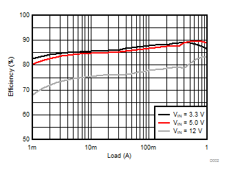
TPS82150 D002_SLVSDN4.gif
Figure 8. Efficiency, VOUT = 1.8 V
TPS82150 D003_SLVSDN4.gif
Figure 10. Efficiency, VOUT = 2.5 V
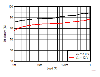
TPS82150 D004_SLVSDN4.gif
Figure 12. Efficiency, VOUT = 3.3 V
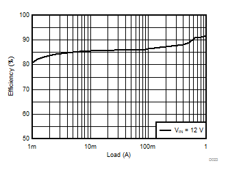
TPS82150 D023_SLVSDN4.gif
Figure 14. Efficiency, VOUT = 5.0 V
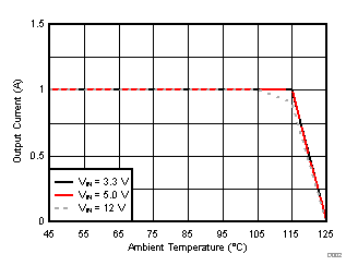
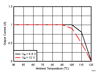
TPS82150 SLVSDN4_thermal_1.0V.gif
θJA = 46.1 °C/W
Figure 16. Thermal Derating, VOUT = 1 V
TPS82150 SLVSDN4_thermal_3.3V.gif
θJA = 46.1 °C/W
Figure 18. Thermal Derating, VOUT = 3.3 V
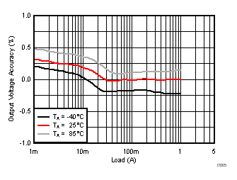
TPS82150 D005_SLVSDN4.gif
Figure 20. Load Regulation
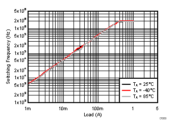
TPS82150 D009_SLVSDN4.gif
VOUT = 1.8V
Figure 22. Switching Frequency
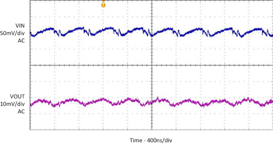
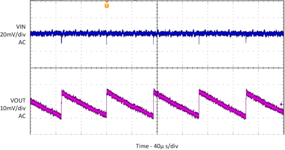
TPS82150 SLVSDN4_PWMripple.gif
IOUT = 1A
Figure 24. Input and Output Ripple in PWM Mode
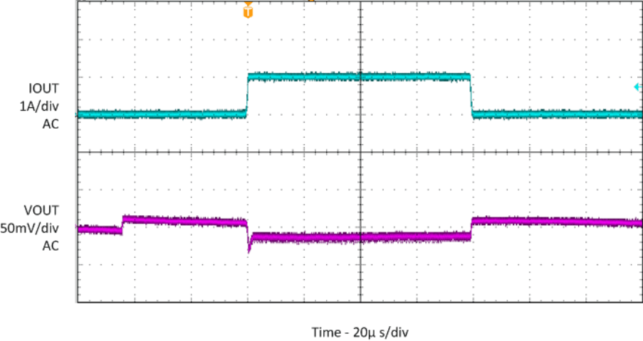
TPS82150 SLVSDN4_loadtran_0to1A.gif
IOUT = 0A to 1A, 1A/µs
Figure 26. Load Transient
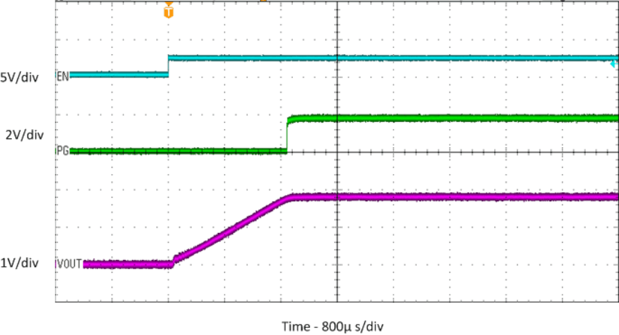
TPS82150 SLVSDN4_startup_noload.gif
No Load
Figure 28. Startup without Load
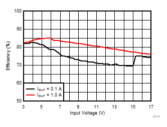
TPS82150 D019_SLVSDN4.gif
Figure 7. Efficiency, VOUT = 1.0 V
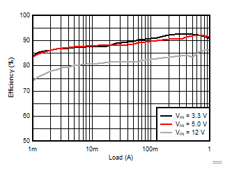
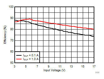
TPS82150 D020_SLVSDN4.gif
Figure 9. Efficiency, VOUT = 1.8 V
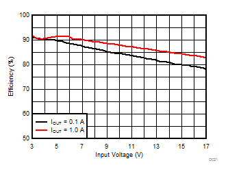
TPS82150 D021_SLVSDN4.gif
Figure 11. Efficiency, VOUT = 2.5 V
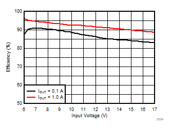
TPS82150 D022_SLVSDN4.gif
Figure 13. Efficiency, VOUT = 3.3 V
TPS82150 D024_SLVSDN4.gif
Figure 15. Efficiency, VOUT = 5.0 V
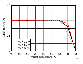
TPS82150 SLVSDN4_thermal_1.8V.gif
θJA = 46.1 °C/W
Figure 17. Thermal Derating, VOUT = 1.8 V
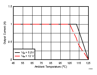
TPS82150 SLVSDN4_thermal_5.0V.gif
θJA = 46.1 °C/W
Figure 19. Thermal Derating, VOUT = 5 V
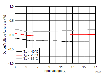
TPS82150 D006_SLVSCY5_TPS82130.gif
IOUT = 1A
Figure 21. Line Regulation
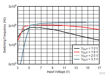
TPS82150 D018_SLVSCY5_TPS82130.gif
IOUT = 1A
Figure 23. Switching Frequency
TPS82150 SLVSDN4_PSMripple.gif
No Load
Figure 25. Input and Output Ripple in PSM Mode
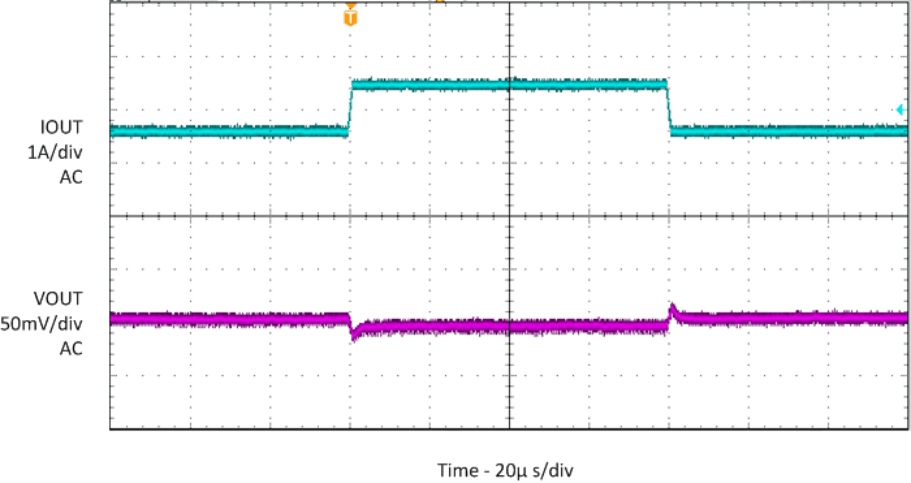
TPS82150 SLVSDN4_loadtran_05to1A.gif
IOUT = 0.5A to 1A, 1A/µs
Figure 27. Load Transient
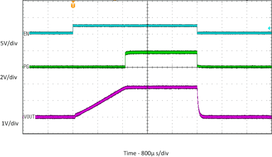
TPS82150 SLVSDN4_startup_1.8Ohm.gif
ROUT = 1.8Ω
Figure 29. Startup / Shutdown with Resistance Load