SLVSCD1C December 2013 – November 2015 TPS92561
PRODUCTION DATA.
- 1 Features
- 2 Applications
- 3 Description
- 4 Revision History
- 5 Pin Configuration and Functions
- 6 Specifications
- 7 Detailed Description
-
8 Application and Implementation
- 8.1 Application Information
- 8.2
Typical Applications
- 8.2.1 Offline Boost Schematic for Design Example
- 8.2.2 11-W, 120-VAC Input, 225-V Output, Offline Boost Design Example
- 9 Power Supply Recommendations
- 10Layout
- 11Device and Documentation Support
- 12Mechanical, Packaging, and Orderable Information
Package Options
Mechanical Data (Package|Pins)
- DGN|8
Thermal pad, mechanical data (Package|Pins)
- DGN|8
Orderable Information
8 Application and Implementation
NOTE
Information in the following applications sections is not part of the TI component specification, and TI does not warrant its accuracy or completeness. TI’s customers are responsible for determining suitability of components for their purposes. Customers should validate and test their design implementation to confirm system functionality.
8.1 Application Information
8.1.1 Setting the Output Current
Using the desired ADJ reference voltage, the input current can be calculated using Equation 3.

where
- VADJ can be DC, rectified AC derived, or other source.
If VADJ is derived from a voltage divider from the input rectified AC, we can solve for the R9 resistor divider value based on, for example, a VADJ voltage of 150 mV, an R17 value of 374 Ω, and the average value of the sine wave:

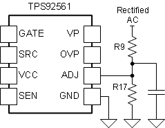 Figure 11. TPS92561 ADJ Connection
To find the RSENSE value, where ƞ is the converter efficiency, assume 0.9.

8.1.2 Selecting an Inductance
The TPS92561 device is hysteretic. Therefore, switching transitions are based on the sensed current in the inductor. There is no direct control of the switching frequency other then the relationship of the comparator hysteresis to the inductor ripple. A typical switching frequency of an off-line converter using a rectified AC injected reference could vary up to 50 kHz over a line cycle. This creates a spread-spectrum effect and helps reduced conducted EMI.
A typical line injected (using a divided down rectified AC as the reference) hysteretic boost converter reaches the peak switching frequency when VLED = 2 × VRECTIFIED AC, or when the duty cycle D = 0.5. We call this operating point VIN-FSW-PK. Use this voltage as the typical operating point for the design equations. Solve for the VIN-FSW-PK term based on Equation 6.

Select the approximate highest desired frequency (for example, fSW-PK of 65 kHz could be used), then design the SEN pin filter with corner frequency equal to fSW-PK. The filter and the internal hysteresis define the inductor ripple for a given inductance. This has the effect of increasing the SEN pin hysteresis VSEN-HYS-2 to approximately 140 mV. Select a C12 value between 1000 and 4700 pF. Solve for the resistor R12 in the filter based on Equation 7.

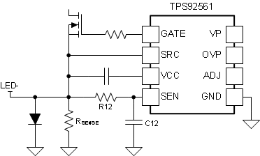 Figure 12. Current Sense
With the effective hysteresis, calculate the inductor peak-to-peak, ΔiL-PP ripple current using:

To find the converter inductance, L, substitute into:

To further aid in the converter design, see the TPS92561 design tool (SLUC517).
8.1.3 Important Design Consideration: Diode in Parallel With Sense Resistance
Figure 12 shows a diode in use in parallel with the RSENSE resistor. The diode clamps the SEN pin voltage when the boost converter is first powered up. Because a boost converter utilizes a diode connected to the output, the output capacitor is charged immediately when power is applied.
CAUTION
The current charging the output capacitor when VIN is applied flows through the sense resistors, and if it is not clamped by the diode, can exceed the TPS92561 SEN pin rating, which may damage the device.
8.1.4 Gate Driver Operation
An additional aid to converter operation and radiated EMI is to slow the main FET switching speed. This can be accomplished by adding a resistor in series with the FET gate. A fast turn off diode across the resistor could also be implemented to improve efficiency. For off-line designs, use a gate resistance value ≥ 75 Ω.
As in all power converters grounding and layout are key considerations. Give careful attention to the layout of the sense resistors, GND pin, VCC, and SRC connections, as well as the FET Gate and Source connections. All should follow short and low-inductance paths. For examples, see the TPS92561 EVM User's Guide, Using the TPS92561 Off-Line Boost LED Driver (SLUUAU9).
8.1.5 Output Bulk Capacitor
The required output bulk capacitor, CBULK, stores energy during the input voltage zero crossing interval and limits the twice the line frequency ripple component flowing through the LEDs. Equation 10 describes the calculation of the output capacitor value.

where
- RLED is the dynamic resistance of LED string
- ILED(ripple) is the peak-to-peak LED ripple current
- fL is line frequency
RLED is found by computing the difference in LED forward voltage divided by the difference in LED current for a given LED using the manufacturer’s VF versus IF curve. For more details, see application report, AN-1656 Design Challenges of Switching LED Drivers (SNVA253).
In typical applications, the solution size becomes a limiting factor and dictates the maximum dimensions of the bulk capacitor. When selecting an electrolytic capacitor, manufacturer recommended de-rating factors should be applied based on the worst case capacitor ripple current, output voltage, and operating temperature to achieve the desired operating lifetime.
8.1.6 Phase Dimming
After following the design procedure for a TPS92561 non-dimming design, the creation of a TRIAC dimmer compatible design only requires the addition of an input snubber (R-C), as shown in Figure 15. Ideally, a capacitor value of 3× the input filter capacitance would be implemented to ensure sufficient damping of the input filter resonance. However, capacitance values as low as 2× tested successfully. If the input voltage is used to provide the converter reference, dimming occurs naturally with the decreasing ADJ set point and decreased power transfer due to shorter line-cycle conduction times.
8.1.7 Example Circuits
Target LED lamp applications include:
- A-15, A-19, A-21, A-23
- R-20, R-25, R-27, R-30, R-40
- PS-25, PS-30, PS-35
- BR-30, BR-38, BR-40
- PAR-20, PAR-30, PAR-30L
- MR-16, GU-10
- G-25, G-30, G-40
Applications also include: fluorescent replacement, recessed (canister) type lighting replacement, and new LED-specific lighting form factors.
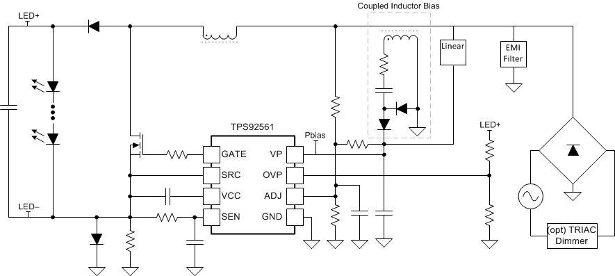 Figure 13. Offline Boost Configuration With Auxiliary Winding and Linear Regulator for Start-Up
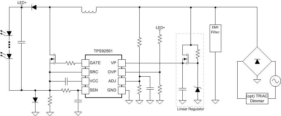 Figure 14. Offline Boost With Linear Regulator from Input Rectified AC
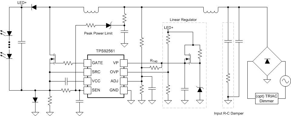 Figure 15. Offline Boost With Linear Regulator from VLED+,THD Improvement Resistor, Peak Power Limit Circuit, EMI Filter, and Snubber for TRIAC Dimming
8.2 Typical Applications
8.2.1 Offline Boost Schematic for Design Example
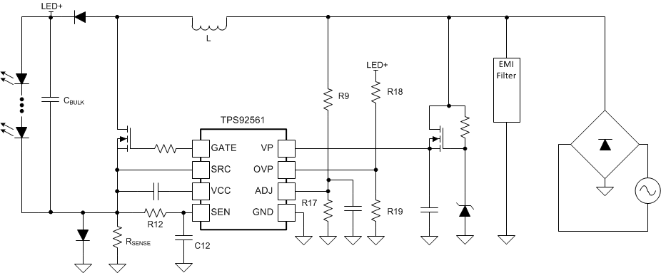 Figure 17. Offline Boost Schematic
8.2.1.1 Design Requirements
- RMS Input Voltage: VIN-RMS
- LED Stack Voltage: VLED
- LED Current: ILED
- LED String Total Dynamic Resistance: RLED
- LED Ripple Current: ILED(ripple)
- Maximum Switching Frequency: fSW-PK
- Over-voltage Protection Level: VOVP
- Approximate Efficiency: η
8.2.1.2 Detailed Design Procedure
8.2.1.2.1 Set the LED Current
8.2.1.2.1.1 Calculate ADJ Pin Resistors
Calculate the ADJ pin resistors by choosing an ADJ voltage and a value for R17. R9 can then be calculated using Equation 11.

8.2.1.2.1.2 Calculate the Current Sense Resistor
The current sense resistor RSENSE can be calculated with Equation 12.

8.2.1.2.1.3 Calculate the SEN Pin Series Resistance
The series resistance between the SEN pin and RSENSE can be calculated by choosing a value of C12 and using Equation 13.

8.2.1.2.2 Calculate OVP Pin Resistors
The OVP pin resistor values can be calculated by choosing a high value for R18 (in the MΩ range) and calculating the value for R19 with Equation 14.

The output voltage falling voltage level for re-start can then be calculated using Equation 15.

8.2.1.2.3 Calculate Inductor Value and Ripple Current
The inductor ripple current is based on the value of RSENSE. The ripple current can be found using Equation 16.

The input voltage where the maximum switching frequency occurs (VIN-FSW-PK) is required for calculating the inductor value and can be found using Equation 17.

Now the inductor value can be calculated using the simplified Equation 18.

8.2.1.2.4 Calculate the Output Capacitor Value
The minimum output capacitor required to meet the LED current ripple requirements can be found using Equation 19.

In this equation fL is the rectified line frequency or double the native line frequency.
8.2.2 11-W, 120-VAC Input, 225-V Output, Offline Boost Design Example
 Figure 18. 11 W, 120-VAC Input, 225-V Output, Offline Boost Schematic
8.2.2.1 Design Requirements
- VIN-RMS = 120 V, 60 Hz
- VLED = 225 V
- ILED = 50 mA
- RLED = 80 Ω
- ILED(ripple) ≤ 25 mA
- fSW-PK = 65 kHz
- VOVP = 250 V
- Approximate Efficiency: η = 0.9
8.2.2.2 Detailed Design Procedure
8.2.2.2.1 Set the LED Current
8.2.2.2.1.1 Calculate ADJ Pin Resistors
Calculate the ADJ pin resistors by choosing an ADJ voltage and a value for R17. Choose an ADJ voltage of 150 mV and a low value of 374 Ω for R17 to get a reasonable value for R9. R9 can then be calculated using Equation 20.

Choose the nearest standard value of R9 = 267kΩ.
8.2.2.2.1.2 Calculate the Current Sense Resistor
The current sense resistor RSENSE can be calculated with Equation 21.

Choose the nearest standard value of RSENSE = 1.43 Ω.
8.2.2.2.1.3 Calculate the SEN Pin Series Resistance
The series resistance between the SEN pin and RSENSE can be calculated by choosing a value of 2.2 nF for C12 and using Equation 22.

Choose the nearest standard value of R12 = 1.1 kΩ.
8.2.2.2.2 Calculate OVP Pin Resistors
The OVP pin resistor values can be calculated by choosing a value for R18 of 1.6MΩ and calculating the value for R19 with Equation 23.

Choose the nearest standard value of R19 = 7.68kΩ. The output voltage falling voltage level for re-start can then be calculated using Equation 24.

8.2.2.2.3 Calculate Inductor Value and Ripple Current
The inductor ripple current is based on the value of RSENSE. The ripple current for this application can be found using Equation 25.

The input voltage where the maximum switching frequency occurs (VIN-FSW-PK) is required for calculating the inductor value and can be found using Equation 26.

Now the inductor value can be calculated using the simplified Equation 27.

Choose the next highest standard inductor value of L = 10mH.
8.2.2.2.4 Calculate the Output Capacitor Value
The minimum output capacitor required to meet 25mA LED current ripple can be found using Equation 28.

In this equation fL is the rectified line frequency of 120 Hz. Choose the next highest standard capacitor value of CBULK = 22µF.
8.2.2.3 Application Curve
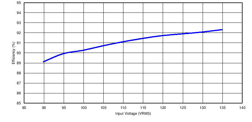 Figure 19. Efficiency vs Input Voltage
