SLVSCD1C December 2013 – November 2015 TPS92561
PRODUCTION DATA.
- 1 Features
- 2 Applications
- 3 Description
- 4 Revision History
- 5 Pin Configuration and Functions
- 6 Specifications
- 7 Detailed Description
-
8 Application and Implementation
- 8.1 Application Information
- 8.2
Typical Applications
- 8.2.1 Offline Boost Schematic for Design Example
- 8.2.2 11-W, 120-VAC Input, 225-V Output, Offline Boost Design Example
- 9 Power Supply Recommendations
- 10Layout
- 11Device and Documentation Support
- 12Mechanical, Packaging, and Orderable Information
Package Options
Mechanical Data (Package|Pins)
- DGN|8
Thermal pad, mechanical data (Package|Pins)
- DGN|8
Orderable Information
7 Detailed Description
7.1 Overview
The TPS92561 device is a boost controller for phase cut dimmer compatible LED lighting applications. The device incorporates a current sense comparator with a fixed offset, allowing the construction of a hysteretic, off-line converter suitable for driving LEDs in a wide variety of applications.
The inductor peak-to-peak current ripple follows the device reference, the ADJ pin voltage (VADJ), and is bounded by the SEN pin hysteresis (VSEN-HYS). By using a voltage divider from the rectified AC voltage, the inductor current can be made to follow the line closely and create conversions which result in high power factor and low THD. Boost converters also have an advantage when TRIAC dimming because of their inherent ability to draw continuous current from the line. This eliminates the need for additional hold current circuitry as the converter itself can draw power until the zero crossing point is reached. The continuous input current of a boost also reduces the input EMI filter requirements.
7.2 Functional Block Diagram
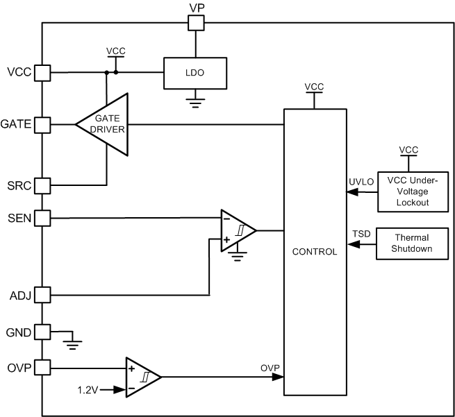
7.3 Feature Description
7.3.1 Basics of Operation
The main switch is turned on and off when the SEN comparator reaches trip points in a window around the ADJ reference. In cycle 1, the main switch is on until the current reaches the turn off threshold. In cycle 2, the switch is kept off until the turn on threshold is reached. In Figure 7, VSEN-UPPER_TH and VSEN-LOWER-TH are assumed to be their typical value of 30 mV.
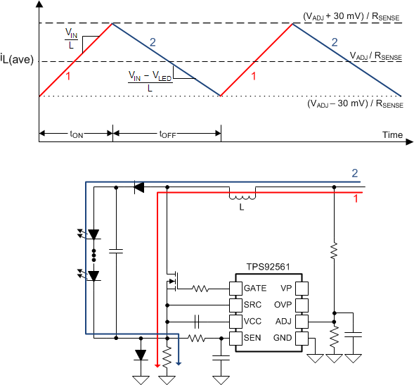 Figure 7. Basics of Hysteretic Boost Operation
7.3.2 Sample Scope Capture
The main inductor current varies in a window around the ADJ reference voltage:
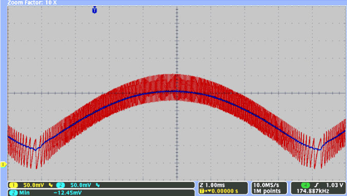 Figure 8. TPS92561 Operation Waveform (1 ms/div)
 Yellow: ADJ Voltage (50 mV/div) Blue: RSENSE Voltage (50 mV/div)
7.3.3 Output Current Control (ADJ, SEN)
The TPS92561 power stage design follows two rules:
- Output current is determined by the ADJ reference voltage, the sense resistor selected, and the converter operating points, VIN and VLED.
- Output frequency is determined by the inductance value and the SEN pin hysteresis VSEN. For off-line applications, the effective hysteresis must be increased using an R-C filter on the SEN pin.
Because the TPS92561 device does not have leading edge blanking, the SEN pin filter must be used to obtain consistent operation. The SEN pin filter is typically set using an R-C with a corner frequency close to the desired switching frequency. Leading edge blanking was not implemented to allow high-frequency operation in other non-off-line applications.
At start up (VADJ < 90 mV) a small current is supplied to the VADJ divider to ensure a reference is available to begin converter switching. When the ADJ voltage is above 90 mV, the current source is shut off.
7.3.4 Overcurrent Protection
The TPS92561 device inherently limits the main switch current, but cannot implement output short circuit protection because of the converter (boost) topology. To implement LED short-circuit protection in a boost converter requires a blocking switch or other means to open the path to the output, which adds significant cost and complexity to the solution and is not commonly used. An input fuse should be used as output overcurrent protection.
7.3.5 Overvoltage Protection (OVP)
Overvoltage protection is implemented using a resistor voltage divider to the output. Note that the output voltage is high (> 200 V) so the resistor divider should contain a high (> 1 MΩ) value. Also use a small cap on OVP.
First pick a value for R18, for example 1.6 MΩ and select the desired overvoltage protection voltage VOVP. Using the VOVP-UPTH value (1.19 V, typical) the trip point can then be computed using:

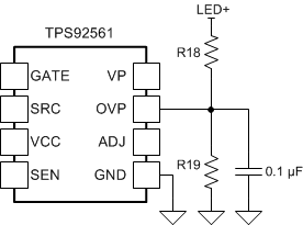 Figure 9. Overvoltage Protection Circuit
When the OVP trip point is reached the converter shuts off until the OVP voltage drops below the level controlled by the OVP hysteresis, VOVP-HYS (44 mV, typical). After OVP is reached, switching begins again when VLED falls to the restart voltage (one VOVP-HYS term ignored):

7.3.6 VCC Bias Supply and Start-Up
The TPS92561 device can be configured to obtain bias power in several different configurations: AUX winding from the main inductor (see Figure 13), a linear regulator from the input rectified AC (see Figure 14), or a linear regulator from the output LED voltage (see Figure 15). A linear regulator can be constructed from a resistor, a Zener diode, and a N-Channel MOSFET. Each configuration has benefits and trade-offs.
Table 1. VCC Bias Power Configurations
| BIAS CONFIGURATION | DESCRIPTION |
|---|---|
| Coupled inductor bias with linear regulator start-up (see Figure 13) |
Highest efficiency bias choice |
| Requires a custom magnetic, which can range in cost similar to an off-the-shelf single coil inductor | |
| Method to start the TPS92561 device (linear) still required, however, can be undersized for start-up condition only. VCCUVLO has not been engineered to support resistive start-up methods. | |
| Linear regulator from output (see Figure 14) |
Lowest efficiency bias choice because output voltage is higher than input |
| Ensures fast output turn off due to bias draining output capacitor | |
| Aids dimming performance under deep dimming, a stable bias is always available | |
| Lower capacitance value required at VP pin, output capacitor is doubling as VP capacitor | |
| Can be supplemented with charge pump bias circuit to achieve higher efficiency | |
| Linear regulator from input (see Figure 15) |
Better efficiency performance than linear regulator derived from output |
| Higher VP capacitor value required |
7.3.7 VCC and VP Connection
A bias voltage with a maximum of 42 V is connected to the VP pin to supply the internal 8.3 V (typical) VCC linear regulator. This voltage is also used to drive the main FET gate. Use a FET with a gate threshold at least 750 mV below the VCC voltage. The VCC capacitor ground must be placed at the SEN pin. This ensures the SEN voltage is free of switching spikes that occur at the edge of each switching cycle.
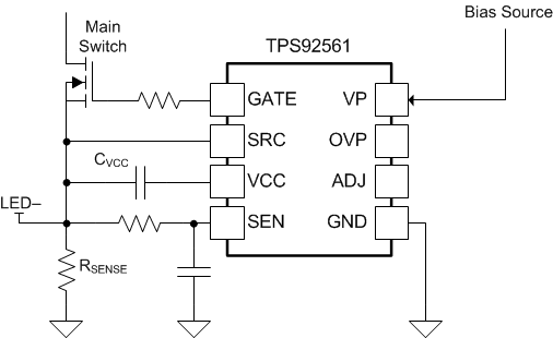 Figure 10. TPS92561 Bias, SRC, and CVCC Connection
7.4 Device Functional Modes
There are no additional functional modes for this device.