SLVSCK5C September   2014  – January 2020 TPS92638-Q1

PRODUCTION DATA.  

  1. Features
  2. Applications
  3. Description
  4. Typical Application Schematic
  5. Revision History
  6. Pin Configuration and Functions
    1.     Pin Functions
  7. Specifications
    1. 7.1 Absolute Maximum Ratings
    2. 7.2 ESD Ratings
    3. 7.3 Recommended Operating Conditions
    4. 7.4 Thermal Information
    5. 7.5 Electrical Characteristics
    6. 7.6 Switching Characteristics
    7. 7.7 Typical Characteristics
  8. Parameter Measurement Information
  9. Detailed Description
    1. 9.1 Overview
    2. 9.2 Functional Block Diagram
    3. 9.3 Feature Description
      1. 9.3.1 LED Current Setting
      2. 9.3.2 PWM Control
      3. 9.3.3 Fault Diagnostics
        1. 9.3.3.1 Open-Load Detection
      4. 9.3.4 Thermal Foldback
    4. 9.4 Device Functional Modes
  10. 10Application and Implementation
    1. 10.1 Application Information
    2. 10.2 Typical Applications
      1. 10.2.1 PWM Dimming by Bank
        1. 10.2.1.1 Design Requirements
        2. 10.2.1.2 Detailed Design Procedure
        3. 10.2.1.3 Application Performance Plots
      2. 10.2.2 Two Brightness Levels for TAIL and STOP Lights
        1. 10.2.2.1 Design Requirements
        2. 10.2.2.2 Detailed Design Procedure
      3. 10.2.3 PWM Dimming by Modulated Supply
        1. 10.2.3.1 Design Requirements
        2. 10.2.3.2 Design Procedure
      4. 10.2.4 Driving LEDs From a Single Device With Channels in Parallel
        1. 10.2.4.1 Design Requirements
        2. 10.2.4.2 Design Procedure
      5. 10.2.5 Driving LEDs From Multiple Devices With Channels in Parallel
        1. 10.2.5.1 Design Requirements
        2. 10.2.5.2 Design Procedure
  11. 11Power Supply Recommendations
  12. 12Layout
    1. 12.1 Layout Guidelines
    2. 12.2 Layout Example
    3. 12.3 Thermal Information
  13. 13Device and Documentation Support
    1. 13.1 Trademarks
    2. 13.2 Electrostatic Discharge Caution
    3. 13.3 Glossary
  14. 14Mechanical, Packaging, and Orderable Information

Package Options

Mechanical Data (Package|Pins)
Thermal pad, mechanical data (Package|Pins)
Orderable Information

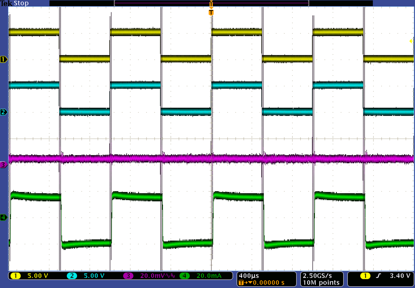
Application Performance Plots

TPS92638-Q1 scope_app1_SLVSCK5.png
SUPPLY = EN = 14 V PWM freq. = 1 kHz Duty cycle = 50%
CH1: PWM1 CH2: PWM2 CH3: Vref
CH4: IOUT8
Figure 39. PWM Dimming by Bank, PWM1, PWM2, Analog Reference and Output Current
TPS92638-Q1 scope_app2_SLVSCK5.png
SUPPLY = EN = 14 V PWM freq. = 1 kHz Duty cycle = 50%
CH1: PWM3 CH2: PWM4 CH3: Vref
CH4: IOUT8
Figure 40. PWM Dimming by Bank, PWM3, PWM4, Analog Reference and Output Current