SLVSCK5C September 2014 – January 2020 TPS92638-Q1
PRODUCTION DATA.
- 1 Features
- 2 Applications
- 3 Description
- 4 Typical Application Schematic
- 5 Revision History
- 6 Pin Configuration and Functions
- 7 Specifications
- 8 Parameter Measurement Information
- 9 Detailed Description
-
10Application and Implementation
- 10.1 Application Information
- 10.2 Typical Applications
- 11Power Supply Recommendations
- 12Layout
- 13Device and Documentation Support
- 14Mechanical, Packaging, and Orderable Information
Package Options
Mechanical Data (Package|Pins)
- PWP|20
Thermal pad, mechanical data (Package|Pins)
- PWP|20
Orderable Information
9.3.3 Fault Diagnostics
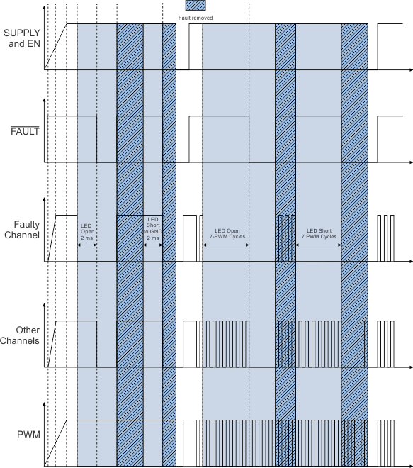
The TPS92638-Q1 device has a fault pin, FAULT, which is for the short, open, and thermal-shutdown general faults. This arrangement allows the maximum flexibility based on all requirements and application conditions.
Connection the device FAULT pin to the MCU allows for fault reporting. The FAULT pin is an open-drain transistor with a weak internal pullup.
The device releases the FAULT bus when external circuitry toggles the FAULT bus, or on a power cycle of the device. In an application that has no MCU, only cycling power clears the fault.
The following faults result in the FAULT pin going low: thermal shutdown, open load, or output short circuit. For thermal shutdown and open LED, release of the FAULT pin occurs when the thermal shutdown or open-LED condition no longer exists. For other faults, the FAULT pin remains low even after the condition does not exist, and clearing is only possible by toggling FAULT or by power cycling of the device.
 Figure 32. TPS92638-Q1 Device Fault-Handling Behavior, FAULT Bus Floating
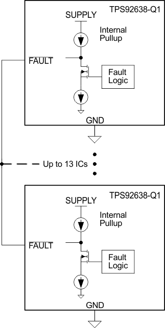
 The design of an application with no MCU allows the connecting together of up to 15 TPS92638-Q1 FAULT̅ pins. When one or more devices have errors, their corresponding FAULT̅ pins go low, thus pulling down the connected FAULT bus and shutting down all device outputs. Figure 33 illustrates the FAULT line bus connection.
 Figure 33. Connection of FAULT Line Bus
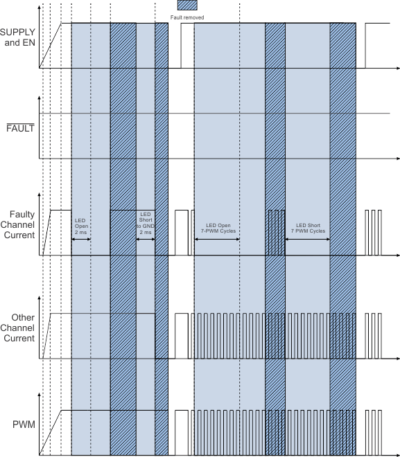
 The device releases the FAULT bus by external circuitry pulling the FAULT bus high, by toggling of the EN pin, or by a power cycle of the device. In an application without an MCU, only a power cycle clears the fault. Figure 34 is a detailed timing diagram.
 Figure 34. TPS92638-Q1 Device Fault-Handling Behavior, FAULT Bus Externally Pulled High
 Table 2. Fault Table
| FAILURE MODE | JUDGMENT CONDITION | DIAGNOSTIC OUTPUT PIN(1) | ACTION | FAULT | DEVICE REACTION | FAILURE REMOVED | SELF CLEARING | ||
|---|---|---|---|---|---|---|---|---|---|
| DETECTION VOLTAGE | CHANNEL STATUS | DETECTION MECHANISM | |||||||
| Short Circuit:
1 or several LED strings |
V(SUPPLY) > 5 V | On | V(IOUTx) < 0.9 V | FAULT | Pulled low | Externally
pulled high |
Failing strings turned off,
other CHs on |
Toggle EN,
power cycle |
No |
| Floating | All strings turned OFF | Toggle EN,
power cycle |
|||||||
| Open Load:
1 or several LED strings |
V(SUPPLY) > 5 V | On | V(SUPPLY) – V(IOUTx) < 100 mV | FAULT | Pulled low | Externally
pulled high |
All strings stay ON | Failure condition removed | Yes |
| Floating | Failing strings stay ON,
other CHs turned OFF |
Failure condition removed | |||||||
| Short to Battery:
1 or several LED strings |
V(SUPPLY) > 5 V | On or off | V(SUPPLY) – V(IOUTx) < 100 mV | FAULT | Pulled low | Externally
pulled high |
All strings stay ON | Failure condition removed | Yes |
| Floating | Failing strings stay ON,
other CHs turned OFF |
Failure condition removed | |||||||
| Thermal Shutdown | V(SUPPLY) > 5 V | On or off | > 170°C | FAULT | Pulled low | Externally
pulled high |
All strings turned OFF | Temperature < 155°C | Yes |
| Floating | |||||||||
| Thermal Foldback | V(SUPPLY) > 5 V | On or off | > 110°C | N/A | None | N/A | Reduced current to all strings | Temperature < 100°C | Yes |
| Reference Resistor Short | V(SUPPLY) > 5 V | On or off | R(ref) < 1400 Ω | FAULT | Pulled low | N/A | All strings turned off | Toggle EN, power cycle | No |