SNVSBT8 March 2021 TPSM13604H
PRODUCTION DATA
- 1 Features
- 2 Applications
- 3 Description
- 4 Revision History
- 5 Pin Configuration and Functions
- 6 Specifications
- 7 Detailed Description
-
8 Application and Implementation
- 8.1 Application Information
- 8.2
Typical Application
- 8.2.1 Design Requirements
- 8.2.2
Detailed Design Procedure
- 8.2.2.1 Design Steps for the TPSM13604 Application
- 8.2.3 Application Curve
- 9 Power Supply Recommendations
- 10Layout
- 11Device and Documentation Support
- 12Mechanical, Packaging, and Orderable Information
Package Options
Mechanical Data (Package|Pins)
- NDW|7
Thermal pad, mechanical data (Package|Pins)
Orderable Information
6.6 Typical Characteristics
FSW = 300 kHz; Cin = 10-μF, X7R ceramic; CO = 47 µF; TA = 25°C (unless otherwise specified)
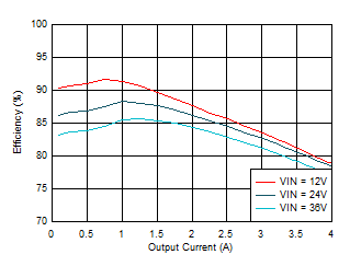 Figure 6-1 Efficiency VOUT = 3.3 V, TA = 25°C
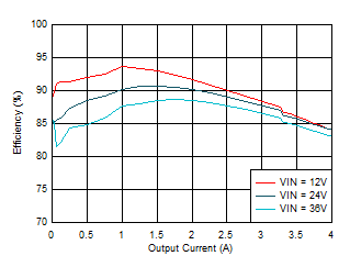 Figure 6-3 Efficiency VOUT = 5.0 V, TA = 25°C
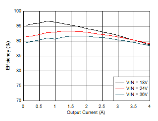 Figure 6-5 Efficiency VOUT = 9.0 V, TA = 25°C
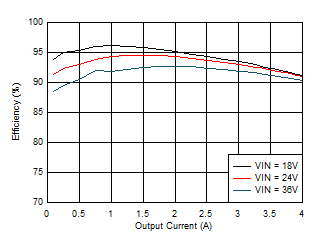 Figure 6-7 Efficiency VOUT = 12 V, TA =
25°C
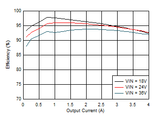 Figure 6-9 Efficiency VOUT = 16 V, TA = 25°C
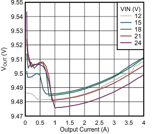 Figure 6-11 Line and Load Regulation VOUT = 9.5 V, TA = 25°C
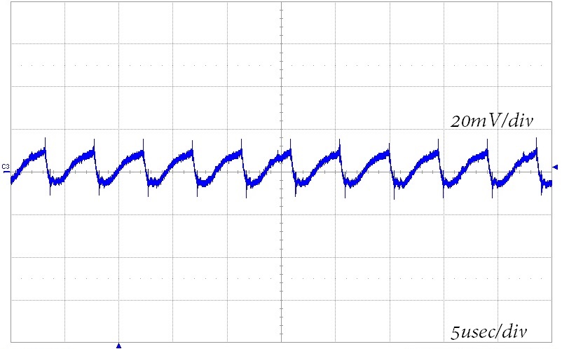 Figure 6-13 Output Ripple
VIN = 12 V, VOUT = 9.0 V, IOUT = 4 A,
Ceramic COUT, BW = 200 MHz
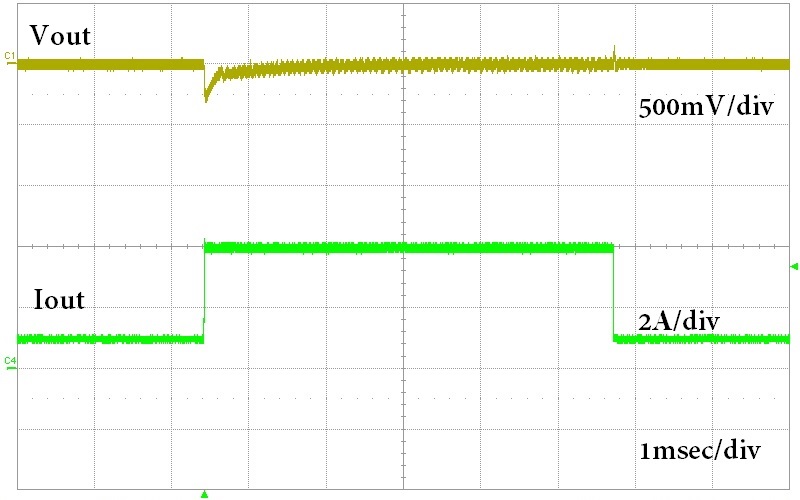 Figure 6-15 Load Transient Response
VIN = 12 V, VOUT = 9.0 V Load Step From 25% to
100%
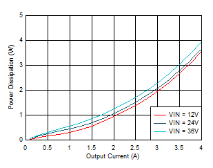 Figure 6-2 Power
Dissipation VOUT = 3.3 V,
 TA = 25°C
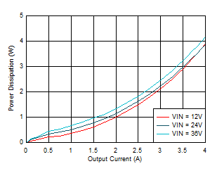 Figure 6-4 Power
Dissipation VOUT = 5.0 V,
 TA = 25°C
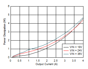 Figure 6-6 Power
Dissipation VOUT = 9.0 V,
 TA = 25°C
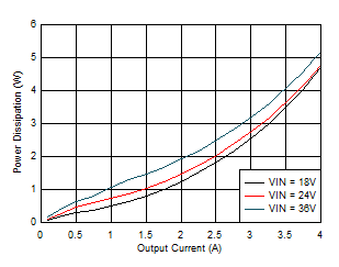 Figure 6-8 Power
Dissipation VOUT = 12 V,
 TA = 25°C
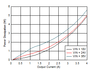 Figure 6-10 Power
Dissipation VOUT = 16 V,
 TA = 25°C
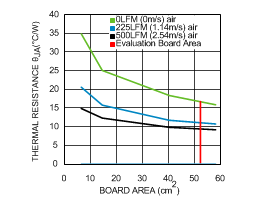 Figure 6-12 Package Thermal
Resistance RθJA
4-Layer PCB with 1-oz Copper
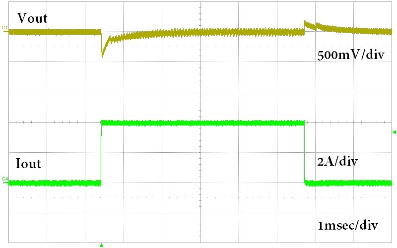 Figure 6-14 Load Transient Response
VIN = 12 V, VOUT = 9.0 V Load Step From 0% to
100%
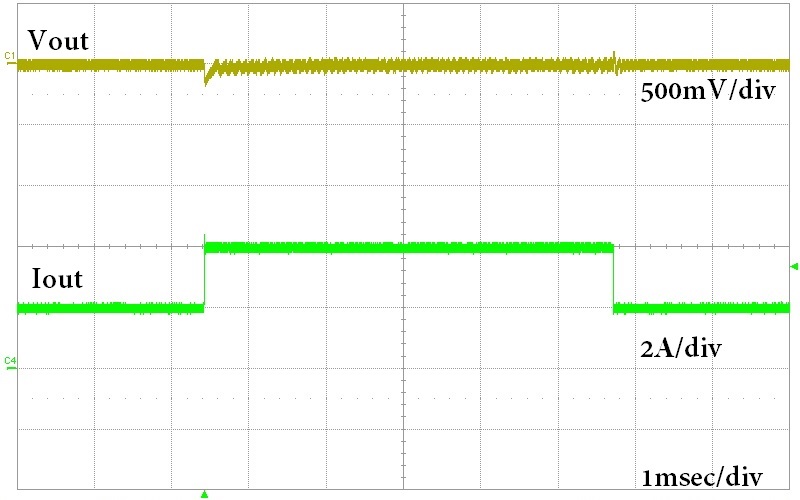 Figure 6-16 Load Transient Response
VIN = 12 V, VOUT = 9.0 V Load Step From 50% to
100%