SNVSBC9C November 2019 – September 2021 TPSM53604
PRODUCTION DATA
- 1 Features
- 2 Applications
- 3 Description
- 4 Revision History
- 5 Pin Configuration and Functions
- 6 Specifications
-
7 Detailed Description
- 7.1 Overview
- 7.2 Functional Block Diagram
- 7.3
Feature Description
- 7.3.1 Adjusting the Output Voltage
- 7.3.2 Switching Frequency
- 7.3.3 Input Capacitors
- 7.3.4 Output Capacitors
- 7.3.5 Output On/Off Enable (EN)
- 7.3.6 Programmable Undervoltage Lockout (UVLO)
- 7.3.7 Power Good (PGOOD)
- 7.3.8 Light Load Operation
- 7.3.9 Voltage Dropout
- 7.3.10 Overcurrent Protection (OCP)
- 7.3.11 Thermal Shutdown
- 7.4 Device Functional Modes
- 8 Application and Implementation
- 9 Power Supply Recommendations
- 10Layout
- 11Device and Documentation Support
- 12Mechanical, Packaging, and Orderable Information
Package Options
Mechanical Data (Package|Pins)
- RDA|15
Thermal pad, mechanical data (Package|Pins)
Orderable Information
7.3.10 Overcurrent Protection (OCP)
The TPSM53604 is protected from overcurrent conditions. Cycle-by-cycle current limit is used for overloads while hiccup mode is used for short circuits. Hiccup mode is activated if a fault condition persists on the output. Hiccup mode reduces power dissipation under severe overcurrent conditions and prevents overheating and potential damage to the device. In hiccup mode, the regulator is shut down and kept off for 94 ms typical before the TPSM53604 tries to start again. If overcurrent or short-circuit fault condition still exist, hiccup repeats until the fault condition is removed. Once the fault is removed, the module automatically recovers with a normal soft-start power up.
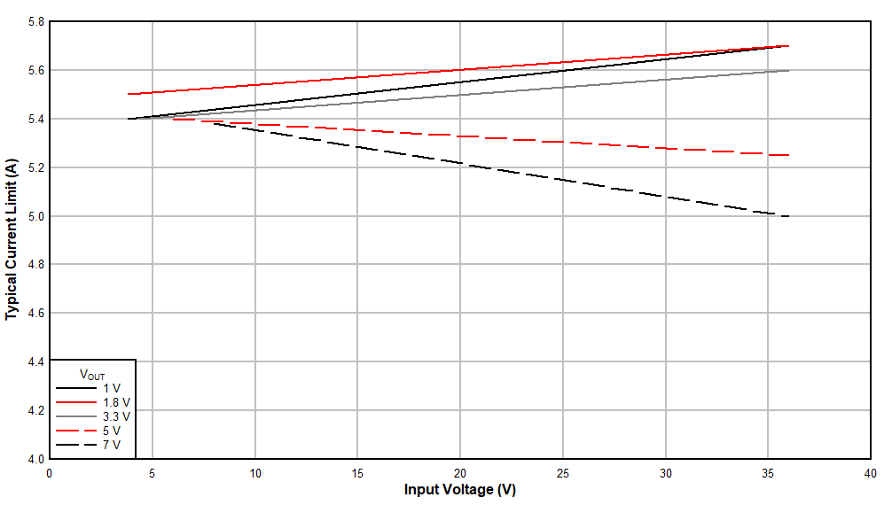
The typical current limit threshold for the TPSM53604 varies slightly as a function of input voltage and output voltage. Figure 7-13 shows the typical current limit threshold for several output voltages over the input voltage range.
 Figure 7-13 Current Limit Threshold