SLUSDV8B November 2020 – March 2021 TPSM5D1806
PRODUCTION DATA
- 1 Features
- 2 Applications
- 3 Description
- 4 Revision History
- 5 Pin Configuration and Functions
- 6 Specifications
-
7 Detailed Description
- 7.1 Overview
- 7.2 Functional Block Diagram
- 7.3
Feature Description
- 7.3.1 Adjustable Output Voltage
- 7.3.2 Frequency Selection
- 7.3.3 Minimum and Maximum Input Voltage
- 7.3.4 Recommended Settings
- 7.3.5 Device Mode Configuration
- 7.3.6 Input Capacitors
- 7.3.7 Minimum Required Output Capacitance
- 7.3.8 Ambient Temperature Versus Total Power Dissipation
- 7.3.9 Remote Sense
- 7.3.10 Enable (EN) and Under Voltage Lockout (UVLO)
- 7.3.11 Soft Start
- 7.3.12 Power Good
- 7.3.13 Safe Start-up into Pre-Biased Outputs
- 7.3.14 BP5
- 7.3.15 Overcurrent Protection
- 7.3.16 Thermal Shutdown
- 7.4 Device Functional Modes
- 8 Application and Implementation
- 9 Power Supply Recommendations
- 10Layout
- 11Device and Documentation Support
- 12Mechanical, Packaging, and Orderable Information
Package Options
Mechanical Data (Package|Pins)
- RDB|51
Thermal pad, mechanical data (Package|Pins)
Orderable Information
7.3.10 Enable (EN) and Under Voltage Lockout (UVLO)
The precision enable feature of the TPSM6D1806 allows the voltage on the EN pin (VEN) to control the ON/OFF functionality of the device. The EN pin has an internal pullup. Floating the EN pin allows the device to start up when a valid input voltage is applied. The TPSM5D1806 switching action and output regulation are enabled when VEN is greater than 1.2 V (typical). While the device is switching, if the EN voltage falls below 1.1 V (typical), the device stops switching.
It is recommended to control the turn ON and turn OFF of the device at a voltage greater than the minimum input voltage as shown in Table 7-2. An external UVLO control can be added using a resistor divider on the EN1 (EN2) pin, between VIN and AGND (see Figure 7-7). Select a top enable resistor of 100 kΩ and calculate the value for the bottom enable resistor (RENB) using Equation 2. It is recommended to use divider resistors with 1% tolerance or better, and with temperature coefficient of 100 ppm or lower.
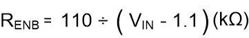
 Figure 7-7 Adjustable UVLO Control